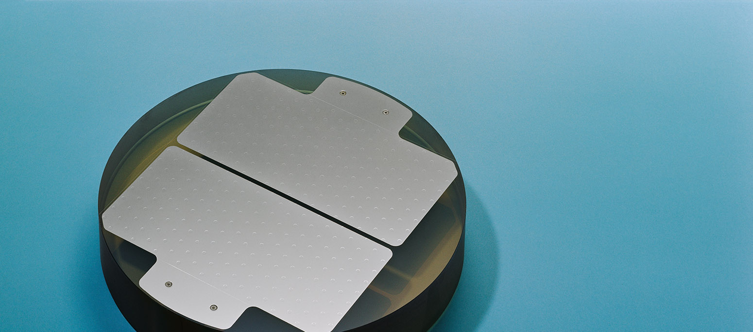
Motivation
Semiconductor substrates such as Si wafers or masks for the next generation of extreme ultraviolet lithography (EUVL) are handled in a vacuum.
For nm structures and exact overlay, the reproducibility of the substrate evenness is a crucial factor, as unevenness results in structural distortions. Particles are problematic and heat input as well as thermal expansion must be taken into account.
Mechanical clamping devices (3-point suspension) cause sagging substrates, abrasion and poor heat contact.
Electrostatic “clamping” to a chuck with “zero expansion” is one alternative. With an electrical voltage between the chuck electrodes, the substrate can be held and, as required, even smoothed.
Benefits
- Substrate holder of highest evenness (< 50 nm PV for chucks for the EUVL masks) with precision manufacturing
- Thermal invariance with “zero expansion” materials
- Electrostatic forces (switchable and adjustable)
- Abrasion and particle generation are negligible
- Pin structured surface minimizes particle risk
- Lightweight design and cooling channels possible
Our work
The Fraunhofer IOF develops electrostatic chucks of the highest evenness for lithography applications. Unipolar and multipolar electrode structures are used:
- Development (CAD/FEM simulation) of next-generation wafer chucks (Si wafers with 450 mm diameter) for 22 nm node and below
- Diameter up to 12 inches
- Vacuum-compatible, non-magnetic
- Chuck materials with minimum (“zero”) thermal expansion
- Surface structuring with honeycomb or pin pattern
- In accordance with SEMI P40
- Kinematic chuck mounting
- Chuck characterization
- Integration in handling and metrology systems
- Sensor integration
