 Fraunhofer Institute for Applied Optics and Precision Engineering IOF
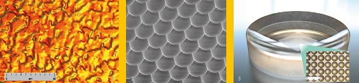
High precision microstructures on various substrates
With outstanding flexibility laserlithography enables for generating high precision microstructures that can be implemented into optical systems. Thus, individual solutions for refractive and diffractive micro optical elements, even on non-standard or non-flat surfaces, can be facilitated in close collaboration with design and integration.
Technical data
- Laserlithography basis system DWL400 from Heidelberg Instruments with modification for freeform exposure
- Exposure at 442 nm wavelength
- 1 μm minimum spot size
- Maximum writing field size: 8 x 8 inch2
- Maximum surface sag: 30 mm
- Maximum surface tilt angle: +/- 10°
- Substrates radius of curvature >10 mm
Realization of micro optical elements
- Calculation, layout and generation of exposure data for various applications
- Fabrication of photo resist structures with laserlithography, e.g. as:
- master for UV replication
- mask for RIE* proportional transfer into the substrate
- mask for structuring functional layers
* RIE – reactive ion etching
Typical applications
- Spherical or aspherical lenses and lens arrays in regular or chirped arrangement
- Beam shaping elements
- Correction of spherical and chromatic aberrations as far as possible directly onto the spherical surface
- Efficient grating und CGHs
- Lithography (also multilayer) on almost every substrate geometry