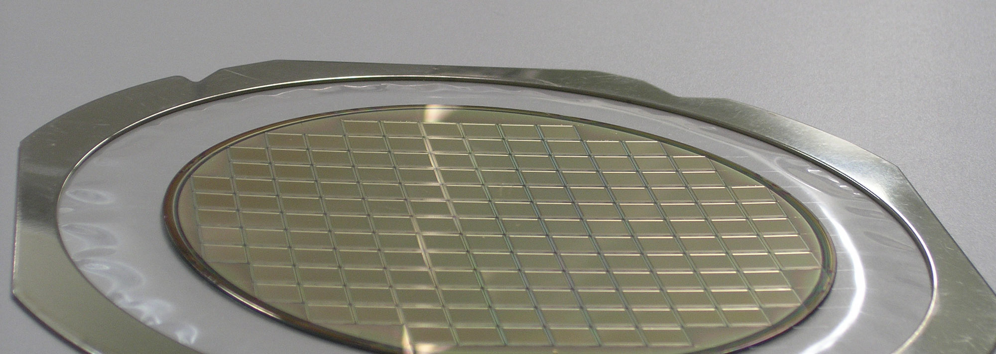
Lithography, dry etching as well as UV molding are characterized by good lateral precision. So the pitch of a lens array can be matched to that of another or to arrays of fibers, detectors, or lasers being a prerequisite for the generation of microoptical systems.
Furthermore, an integration on wafer scale becomes feasible
Typical examples are the following
- UV molding on top of a wafer carrying detectors or VCSELs
- Multifunctional elements fabricated by combination of technologies
- Double sided UV molding in a mask aligner
- Double sided elements fabricated by dry etching
- Surface coating; this involves anti-reflection coatings, but also the integration of filters, beam splitters etc.
- Generation of electrode patterns
- Integration of apertures made with metal as well as with black polymer
As the last process step the wafer can be separated into a high number of micro-optical (sub-)systems.
