Jena / February 21, 2023
New features for silicon photonics
New Fraunhofer-Attract project SILIQUA aims to develop silicon-based photonic devices with enhanced functionalities
Researchers at the Fraunhofer Institute for Applied Optics and Precision Engineering IOF want to investigate how silicon-based photonics technologies can be equipped with new functionalities as part of the SILIQUA project. In doing so, they are paving the way for cheaper, faster, and more powerful technologies, for example in communication and data processing, but also in sensor technology. The project has now started and is funded within the Fraunhofer Attract program.
Silicon is a frequently used material in semiconductor and chip manufacturing. Researchers at Fraunhofer IOF now want to develop a new generation of active silicon photonic devices that can be integrated into existing electrical and optical chip technologies, where they can perform novel functions. This is the goal of the research project SILIQUA ("Silicon-based Photonic Building Blocks for On-Chip Lighting, Modulation, Sensing and Quantum Applications"), which has now started at Fraunhofer IOF in Jena.
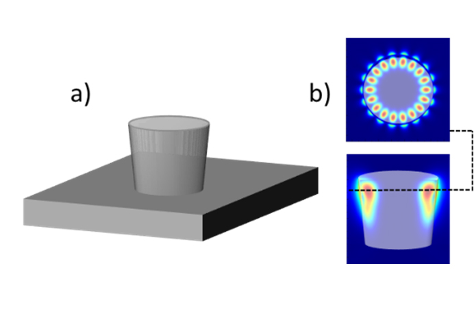
The work will focus in particular on the development and production of infrared light sources as well as modulators and sensors. First, photonic waveguide architectures and resonators will be developed in which light waves are guided on the chip. These will be functionalized with electro-optically active or optical non-linear coatings or defects, respectively, and can then be used as versatile components for novel photonic silicon LEDs, lasers, quantum light sources, modulators, and sensors. In the process, the design and processes in the fabrication of the components will be optimized using machine learning methods.

Enormous growth of silicon-based photonic technology
In the past decades, silicon-based photonic technologies have experienced explosive growth. In addition to already technologically mature solutions, for example in the field of on-chip communication or biochemical sensor technology, particular progress has recently been made in complex optics such as photonic quantum processors in which all the necessary components such as light sources, modulators and detectors are integrated on a single chip.
These integrated optics, also known as "photonic integrated circuits" (PICs for short), are characterized by particularly high functionality. Technology platforms consisting of different material systems are used in the manufacture of these PICs. Among these, the silicon platform is unique because it is based on already established manufacturing technologies and therefore enables new functionalities to be easily introduced to the market. It is compatible with the dominant CMOS ("Complementary Metal-Oxide-Semiconductor") technology in microelectronics, allowing the simultaneous integration of electrical and optical functionalities. Furthermore, the silicon platform is largely independent of rare and expensive materials and therefore allows a large added value for manufacturers and reduces their strategic dependencies.
Fields of application in the areas of communication and security
The integration of silicon resonators in lasers, quantum light sources, or sensors opens up numerous fields of application in the areas of communications and security, consumer electronics, mobility, and space travel. For example, faster cell phones and computers can be produced that fulfill new functions and can also be produced in an energy- and cost-efficient manner. Far beyond that, the newly developed silicon PICs can also be useful for applications in quantum computing or telecommunications.
The project is coordinated by Fraunhofer IOF. In addition, the researchers are cooperating in various disciplines with the University of Jena, the Helmholtz Centers in Berlin and Dresden, and with the Oak Ridge National Laboratory in Tennessee.
The project is funded by the Fraunhofer-Gesellschaft as part of the Fraunhofer Attract funding program. A total of 2.5 million euros in research funding is flowing into the project, which is supported in equal parts by the Fraunhofer IOF and the Fraunhofer-Gesellschaft.
About the Fraunhofer-Attract funding program
The Fraunhofer-Attract funding program enables researchers to further develop their ideas in an application-oriented manner. The funding is intended to enable external scientists to transfer their research into application within a Fraunhofer institute at the interface between science and industry.