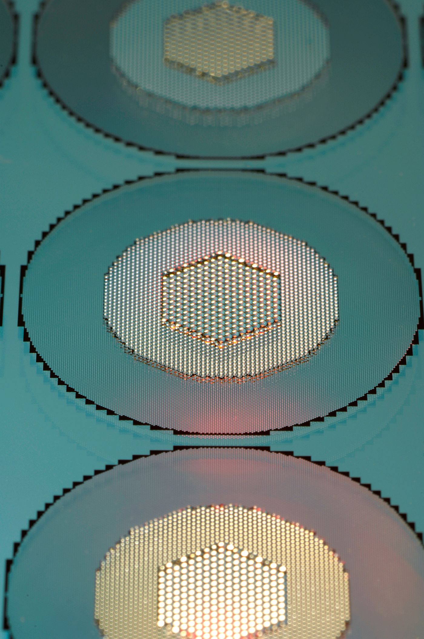
Objective
Reproducible fabrication of refractive microlenses with parameters derived from system design calculations.
Technology
- Mastering by direct-writing grayscale lithography or binary mask lithography and reflow
- Replication by UV polymer molding or
- Transfer to silicon, glass or fused silica by reactive ion etching
- AR-coating, dicing
- Integration of aperture- / filter structures
- Double-sided patterning (tandem arrays)
Geometry of the lens arrays
- Spherical, cylindrical or elliptical lenslets; sag up to 100 μm
- Layout and focal length varying across the array / wafer („Chirp”)
- Lens diameter: 5 μm – 3000 μm
- Resolution / lens gap: 1 μm
- High fill factor, lateral precision
- Homogeneity of focal lengths: ±1 % across wafer
- Generation of aspheres by reactive ion etching (RIE)
- 100% fill factor of arrays by RIE assisted mastering
Replication by UV molding
- As thin polymer layer on glass, Si, etc.
- High lateral and axial precision
- High chemical / thermal stability
- On top of processed wafers (CMOS, VCSEL)
Applications
- Laser / fiber collimation
- Beam forming elements, homogenizer
- Fill factor enhancement on detector arrays
- Field-of-view matching for displays
- Miniaturized imaging systems, sensors
