Electron beam lithography enables compact design of novel components for quantum technologies
Twelve million euros for new system for high-performance optics made in Jena
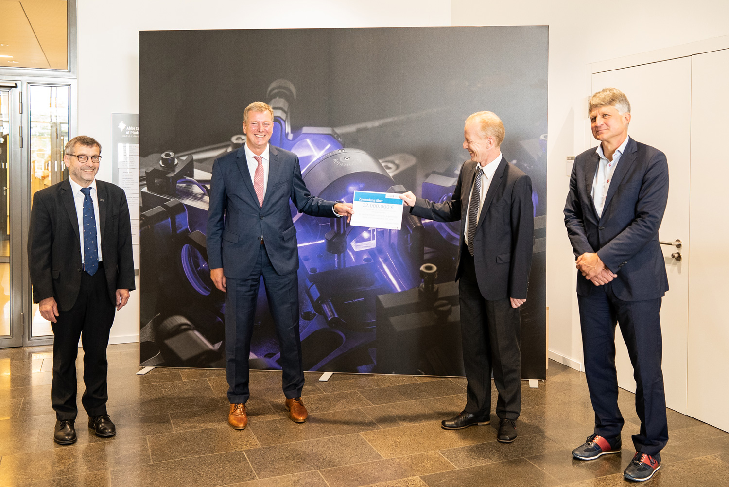
The Thuringian Ministry of Economics and Science is supporting the acquisition of a new lithography system at the Fraunhofer Institute for Applied Optics and Precision Engineering IOF in Jena with twelve million euros. The new system will enable outstanding basic research in the field of quantum technologies. It will also enable the realization of optics, e.g. for the space-borne observation of climate change. State Secretary Carsten Feller presented the funding decision today.
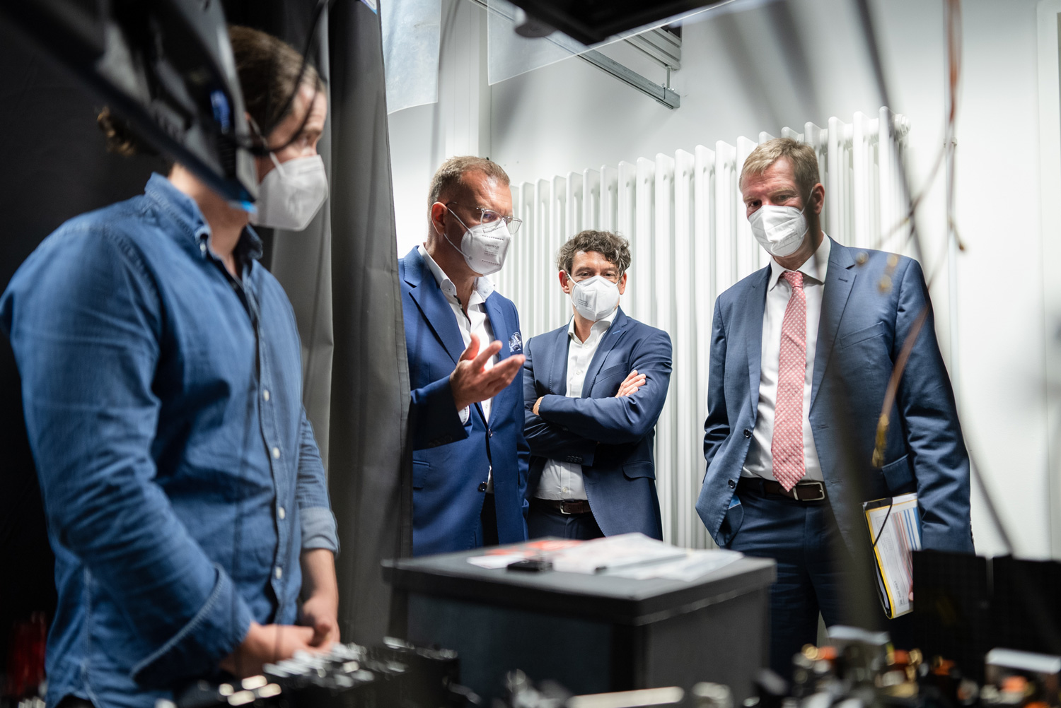
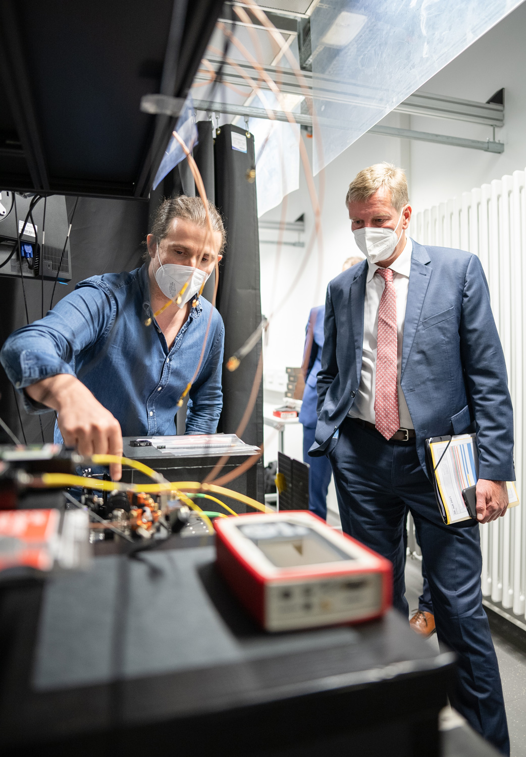
When these days research is conducted on quantum technologies at the Fraunhofer IOF laboratories, researchers need quite a bit of space for it: Entire lab benches are currently taken up by the optical setups. This is too large for the commercialization of quantum technologies and their practical application in everyday life. A reduction, to the size of a chip for example, is therefore unavoidable. Such miniaturization can be achieved with certain manufacturing processes for high-performance optics. "Electron beam lithography" is such a process.
Pioneer in Germany and the EU
"The new electron beam lithography system at Fraunhofer IOF secures a unique global position for Thuringia in the manufacture of nano- and micro-optical components," emphasized State Secretary Feller on the occasion of his visit to the institute today and the handover of the funding decision. "It is another milestone for the research and development of quantum technologies and thus for the positioning of Thuringia as a pioneer in this field in Germany and the EU." For several years now, the state has been supporting the Fraunhofer IOF in establishing infrastructures for quantum research and development of solution approaches for industry. Applications such as quantum computers or analysis and measurement technology with quanta put conventional systems far in the shade, Feller continued.
The acquisition of the new system thus continues the momentum of recent investments in the field of quantum research: Only in May, a new research network for quantum technologies opened in Thuringia with the "Quantum Hub Thüringen". The new research building of Fraunhofer IOF, which is currently under construction, will also provide new space for quantum research.
A new level for quantum technologies and spectroscopy
Beyond applications in the field of quantum technologies, the system will enable a new, significantly more powerful generation of high-performance optics, e.g. for space-based earth observation. These are indispensable for climate monitoring and thus for studying the effects of global climate change. However, there is also dormant potential for applications in other areas of spectroscopy, e.g. in the analysis of food or pollutants.
“Our new system will substantially expand Fraunhofer IOF's capabilities in the field of micro- and nanostructure generation and enable us to advance into completely new areas of structuring precision, resolution, speed, and component size,” explains Uwe Zeitner, who is responsible for investments and infrastructure at Fraunhofer IOF. Together with his colleagues, he is planning the system and working with partners from industry to ensure that it can go into operation in 2023. “Fraunhofer IOF will thus become an ’enabler’ for making future high-performance optics even more accurate than we can do today,” Zeitner continues.
Tiny structures with high resolution
The tiny structures of high-performance optics remain hidden from the human eye and yet they have a decisive influence on the performance and potential application of optics. They are half a thousandth of a millimeter in size. By comparison, a human hair has a diameter of up to 0.1 millimeters. These small optical components can achieve functions that cannot be generated with conventional lenses, such as those known from eyeglasses or a camera lens.
But in order to use these tiny structures, they not only have to be designed and developed, but also written onto a so-called “carrier”. How can you do that with such small structures? Various techniques can offer a solution to this question. One of them is electron beam lithography, which operates particularly precisely and thus permits an exceptionally high resolution. It works in a similar way to writing on a sheet of paper with a high-precision typewriter. However, instead of ink, it uses electrons. And these electrons are much smaller than any drop of ink.
The ability to generate functional photonic micro- and nanostructures with high precision is a key technology and paves the way for numerous applications in core markets of German industry such as energy, health, mobility, and production. With the new system, Fraunhofer IOF will continue to advance applied research in these fields, which are important for our society.
Innovation driver in the field of high-performance components
With its “Center for Advanced Micro- and Nano-Optics”, established in 2006 with funds from the Free State of Thuringia, Fraunhofer IOF already plays a leading role worldwide as an innovation driver in the field of high-performance components for various micro-optics applications. “In order to successfully occupy this leading position in the field of high-end applications of optical micro- and nanostructures in the future, a strategic renewal of the technological platform at Fraunhofer IOF with an electron beam lithography system as a central starting point is extremely important”, Uwe Zeitner says, explaining the necessity of the new acquisition.
“In addition, the new technology platform will also lay the foundations for German companies to address new markets and conduct unique experiments of basic and applied research,” Zeitner adds.
Perspectives for further cooperation at the optics location Jena
The new system is also intended to strengthen cooperation with other scientific institutions at the optics location Jena. Together with the Institute of Applied Physics (IAP) of the Friedrich Schiller University of Jena and the Leibniz Institute of Photonic Technology (IPHT), it will provide a basis for further successful joint research projects.
When the new system is available at the institute, which is expected to be in 2023, it will be installed in a new institute building. This is necessary in order to meet the increased requirements of the system and all manufacturing processes in the development of high-performance optics.
Last modified:


