The Fraunhofer IOF has state-of-the-art process chains for optical components and systems, from design and manufacturing to system integration. Applications cover the entire spectral range from EUV to THz.
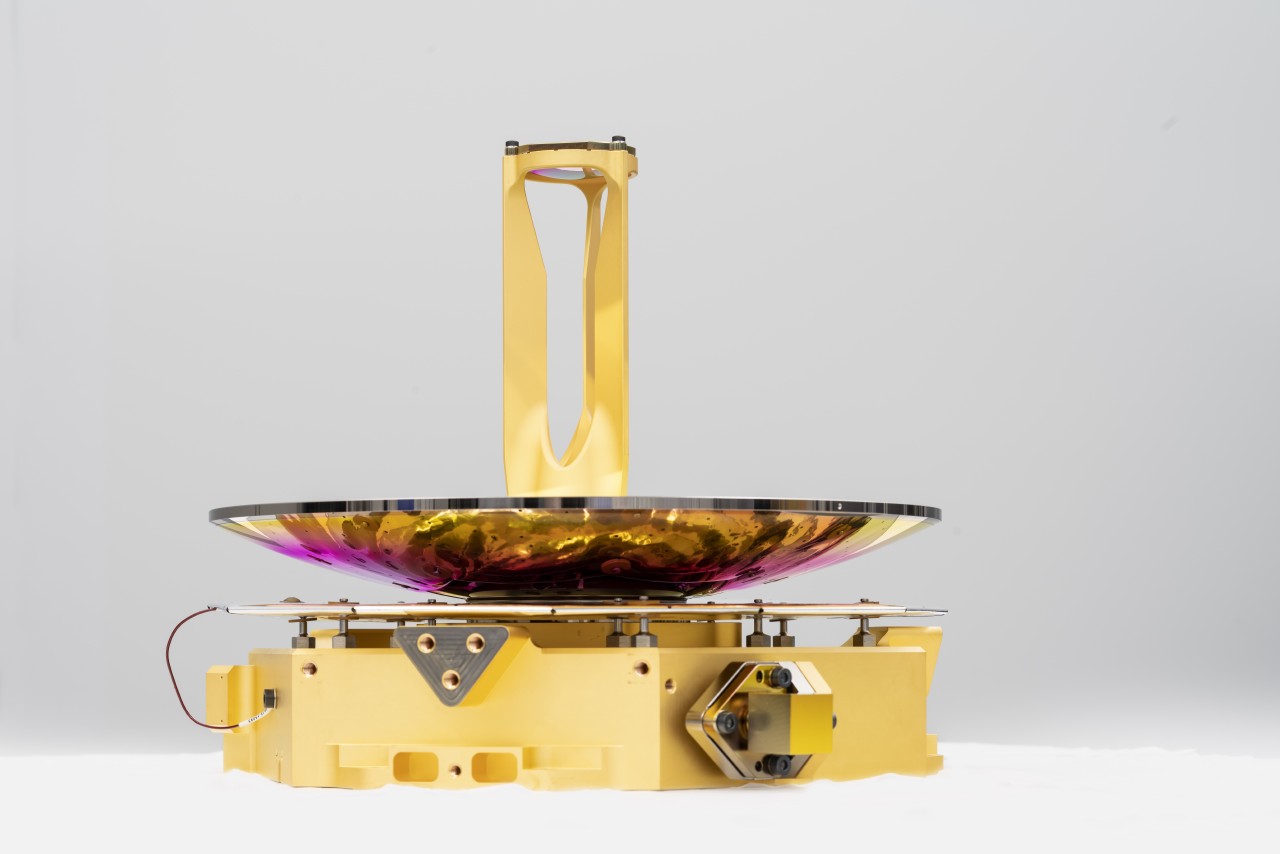
In addition to the production of conventional aspherical optics, the Fraunhofer IOF develops modern free-form optics and adaptive optics up to 500 mm in diameter. Micro- and nanostructures for future photonic applications are realized on the basis of high-resolution lithographic technologies.
The technology chains can be combined in hybrid form.
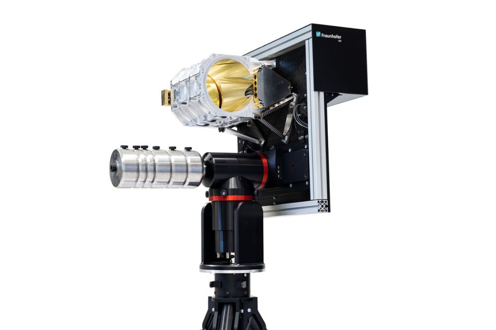
The main areas of focus are in the fields of instrumentation for space/astro systems, equipment for lithography systems, micro- and nano-optical components, as well as optical security and communication systems.


