Research Reports: Atomic Layer Deposition

Recent ALD developments at Fraunhofer IOF

Fraunhofer IOF offers a wide range of functionalizations of surfaces and layers. One technology used and further developed by our experts is atomic layer deposition (ALD). This process enables conformal thin film growth of organic or also hybrid organic-inorganic coatings on nano-/microstructured substrates as well as on freeform and strongly curved surfaces.


Could ALD be a solution for your coating problem?

Find out about our technologies, licenses, and range of services for customers from industry and science by clicking here:

Conformal coating with ALD


Below you will find research reports on our recent ALD developments:

Atomic Layer Deposition of Antireflection Coatings and Bandpass Filters.
© Fraunhofer IOF
Conformal coatings are enabled by atomic layer deposition (ALD). It allows precise thickness and composition control of thin films on arbitrarily shaped optics, which is a prerequisite for high optical performance.

Conformal coating for high-efficiency spectrometer gratings

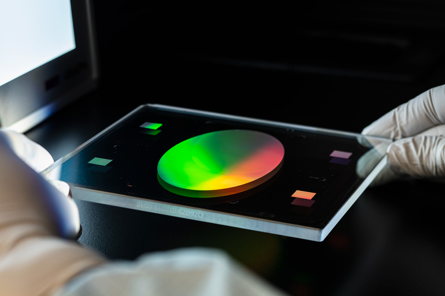
With ALD coated spectrometer grating in the hands of a researcher.
© Fraunhofer IOF
The atomic layer deposition process enables conformal coating even for diffraction gratings.


High-efficiency diffractive gratings, which comprise the key components of earth-monitoring spectrometers in the NIR/SWIR spectral range as dispersive elements, impose great challenges on the manufacturing process. At Fraunhofer IOF, in cooperation with the scientific department "Micro- and nanostructured optics", a high and nearly polarization-independent diffraction efficiency is achieved by embedding a fused silica grating into a high refractive index material (TiO2) and an antireflective SiO2 top layer (Fig. 1).

High quality, homogenous, and void-free coatings are required for high efficiency. The embedding is therefore done by atomic layer deposition (ALD), which can deposit conformal coatings onto deep gratings. The continuously increasing aspect ratio of the grooves is a particular challenge for their filling; thus, the deposition process must be optimized for such gratings. In addition, the refractive index and the coating thickness must be controlled precisely.

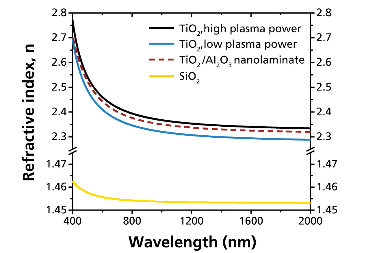
In this holistic approach, the optimization of process parameters (precursor material, dose and purge times, plasma conditions etc.) for the specific grating has been performed. Plasma-enhanced ALD (PEALD) processes enable TiO2 coatings with a high refractive index. However, these coatings have a high roughness at the film thickness required for filling the grooves of above 300 nm. Smooth coatings are obtained by TiO2/Al2O3 nanolaminates (AFM roughness, RMS < 1 nm). In addition, the refractive index can be adapted to the optimal grating design by adjusting the amount of Al2O3 in the nanolaminate. Controlling  the ratio of the components in the nanolaminates and the plasma conditions allows a refractive index of 2.32+/-0.01 @ 2 μm (Fig. 2). Thus, transmission gratings with an average diffraction efficiency above 90 % and a polarization sensitivity below 4 % have been demonstrated for the SWIR2 channel in the 1900 nm to 2095 nm spectral range.


Embedded grating with ALD coating.
© Fraunhofer IOF
Fig. 1: Embedded grating with ALD coating.
Dispersion curves of SiO2 and TiO2 thin films and TiO2/Al2O3 nanolaminate.
© Fraunhofer IOF
Fig. 2: Dispersion curves of SiO2 and TiO2 thin films and TiO2/Al2O3 nanolaminate.


Authors: Kristin Pfeiffer, Vivek Beladiya, Torsten Harzendorf, Thomas Flügel-Paul, Adriana Szeghalmi


Further research reports on ALD


The articles listed below underline, among other things, the intensive research activities of our experts at Fraunhofer IOF. These articles are published in our annual reports, which contain selected research results from the corresponding years (archive annual reports).

In the following list you will find the articles on developments regarding atomic layer deposition from the past years:


HfO2 and SiO2 ALD coatings for laser applications

Atomic layer deposition coatings on complex substrates.
© Fraunhofer IOF
Atomic layer deposition coatings on complex substrates.


Interest in applying strongly curved lenses to laser systems is increasing. However, many of these lenses cannot be functionalized properly because established coating technologies lead to thickness gradients along the surface of the lens.

Atomic layer deposition (ALD) allows uniform and conformal thin films with a precise thickness control on arbitrarily shaped optics to achieve a high optical performance along their surface. Thin ALD functional optical coatings and nanoporous SiO2 layers have been demonstrated as broadband and wide-angle antireflection coatings or as  single-layer antireflection coatings with a high laser-induced damage threshold.

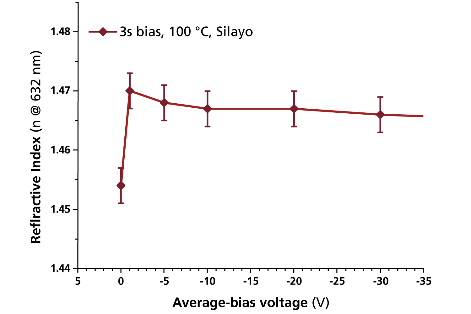
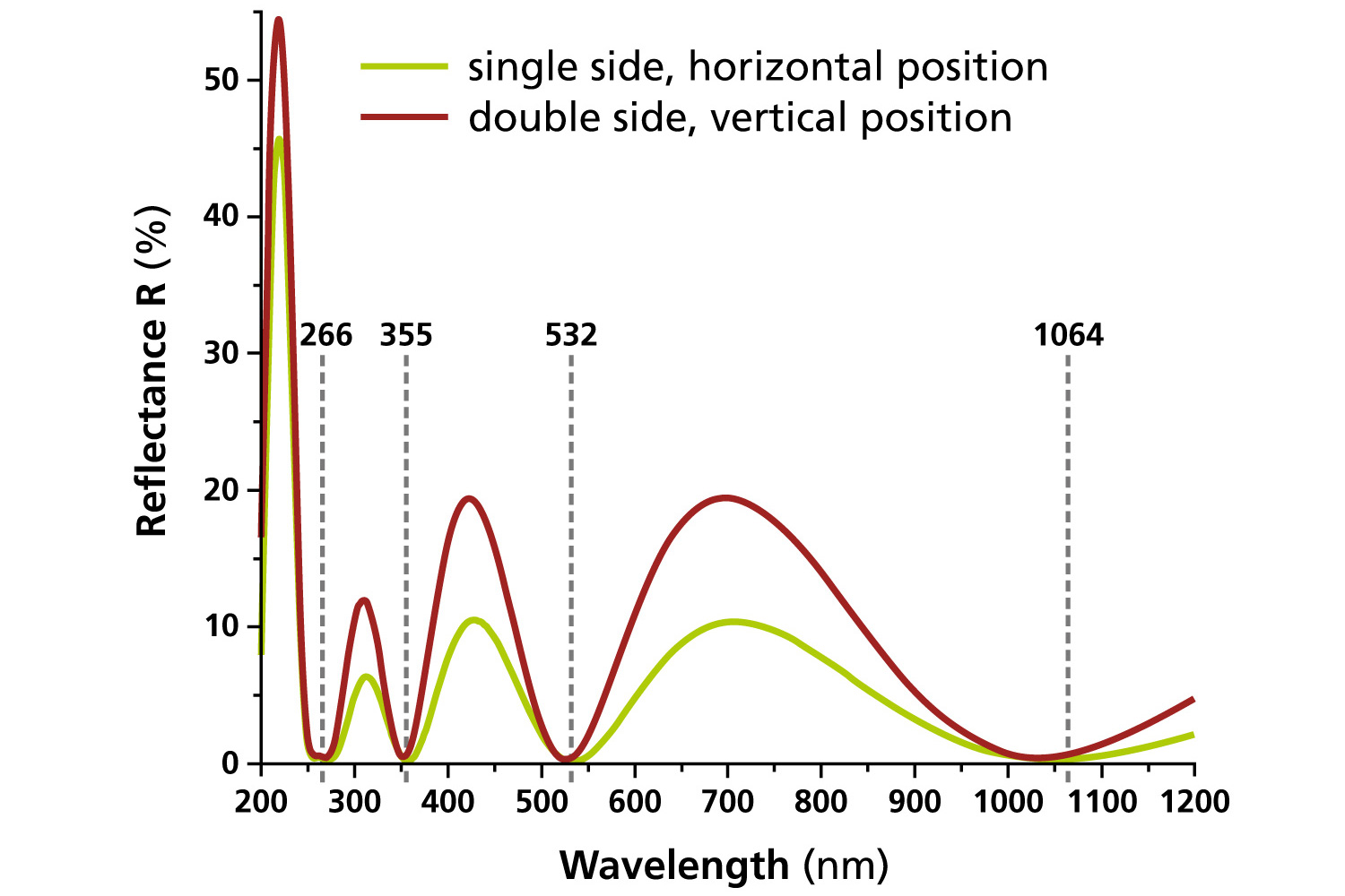
At Fraunhofer IOF, a large-scale plasma-enhanced ALD (PEALD) tool for the deposition of oxides and nitrides on substrates with a diameter of up to 330 mm and a height up to 150 mm has been installed. Thin films of SiO2, Al2O3, TiO2, and HfO2 can be grown with very good uniformity at a low deposition temperature (100 °C). Additionally, the optical and mechanical properties of the coatings can be tailored by applying a bias voltage. Figure 2 shows the refractive index of SiO2 thin films as a function of the applied bias voltage. Coatings with superior quality are obtained already at a very low bias voltage. A multilayer interference coating is demonstrated for antireflection coatings of fused silica substrates at 1064, 532, 355, and 266 nm wavelength for laser applications.


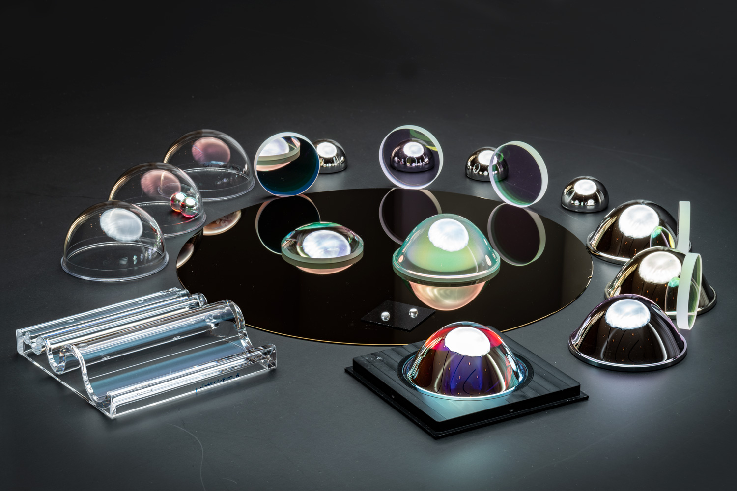
Different curved optical components coated with ALD.
© Fraunhofer IOF
Fig. 1: Atomic layer deposition (ALD) can be used for coating optical components such as aspheres, convex and concave lenses, or ball lenses.
Chart with refractive index of SiO2 ALD thin films as a function of the bias voltage.
© Fraunhofer IOF
Fig. 2: Refractive index of SiO2 ALD thin films as a function of the bias voltage.
Chart with reflectance from one side and from both sides of a fused silica substrate with an antireflection multilayer system.
© Fraunhofer IOF
Fig. 3: Reflectance from one side and from both sides of a fused silica substrate with an antireflection multilayer system.


Authors: Vivek Beladiya, Margarita Lapteva, Adriana Szeghalmi

Properties of oxides on a new PEALD coating system

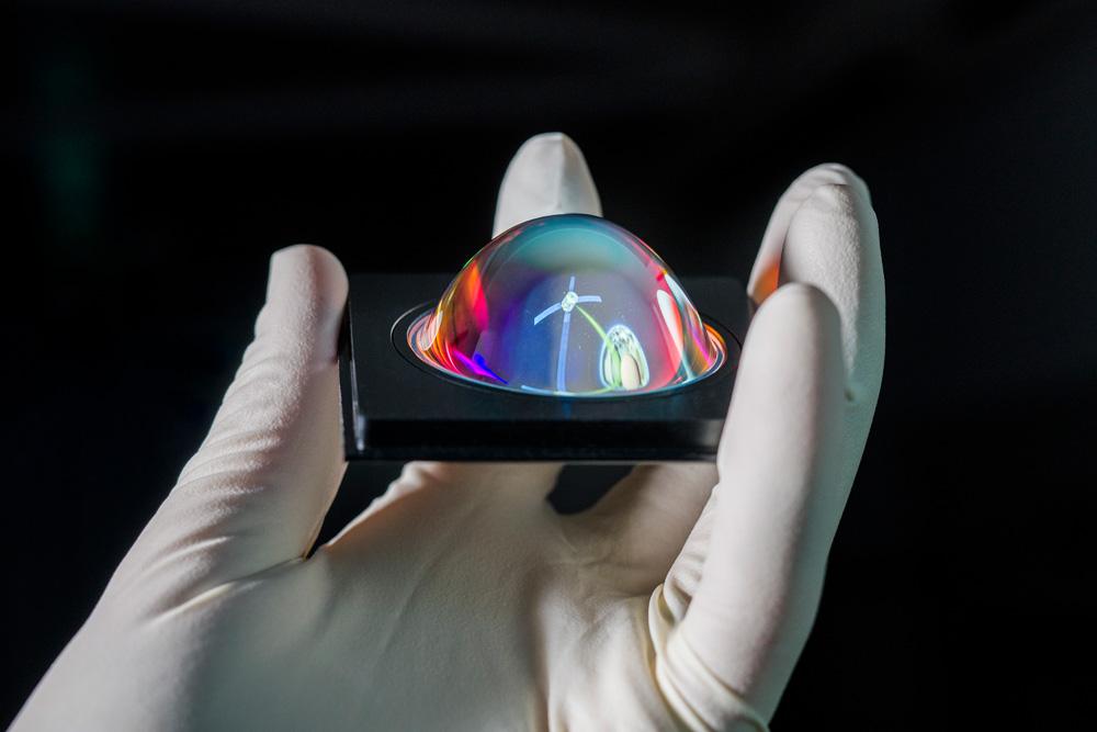
With ALD coated half-ball lens in the hand of a researcher.
© Fraunhofer IOF
A half-ball lens functionalized with ALD.


The deposition of uniform and conformal thin films with a precise thickness control is essential for the development of optical components with a complex topography. Atomic Layer Deposition (ALD) is a key technology in the semiconductor industry for coating high aspect ratio nanostructures. This technology is also attracting increasing interest for optical applications. Thin ALD coatings are applied in interference multilayer systems (Fig. 1) and gratings.

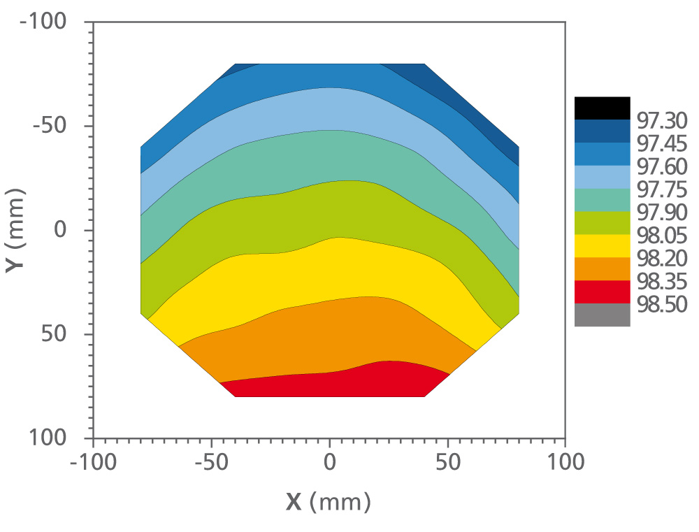
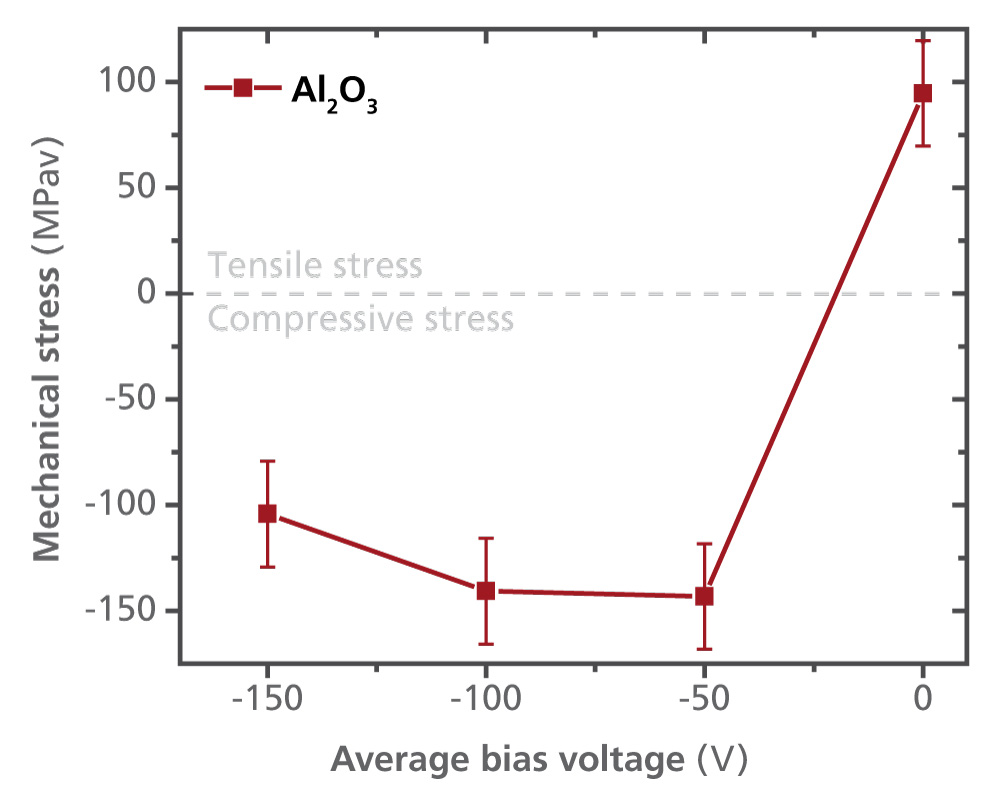
The newly installed plasma enhanced ALD (PEALD) tool allows the deposition of oxides and nitrides on substrates with a diameter of up to 300 mm and a height up to 100 mm. The Planar Triple Spiral Antenna (PTSA) of the equipment is an inductively coupled plasma (ICP) source with a diameter of 400 mm. It enables high film thickness uniformity. In addition, a bias voltage can be applied to the substrate during the deposition to tailor the optical and mechanical properties of the coatings. The developed processes for SiO2, Al2O3, and TiO2 were optimized at a substrate temperature of 100 °C to 250 °C. The film thickness uniformity ( (dmax-dmin) / 2daverage ) achieved across a 200 mm diameter area is ± 0.3 % (Al2O3), ± 0.8 % (TiO2), and ± 0.6 % (SiO2), see Figure 2. Standard Al2O3 films with film thickness of 200 nm show 97 MPa tensile stress. In contrast, Al2O3 films show compressive film stress between 109 MPa and 144 MPa when a bias voltage was applied during deposition (Fig. 3).

The goal is the development of optical elements, such as dichroic mirrors and narrow bandpass filters, with low residual stresses to avoid crack formation and delamination.


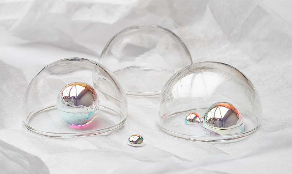
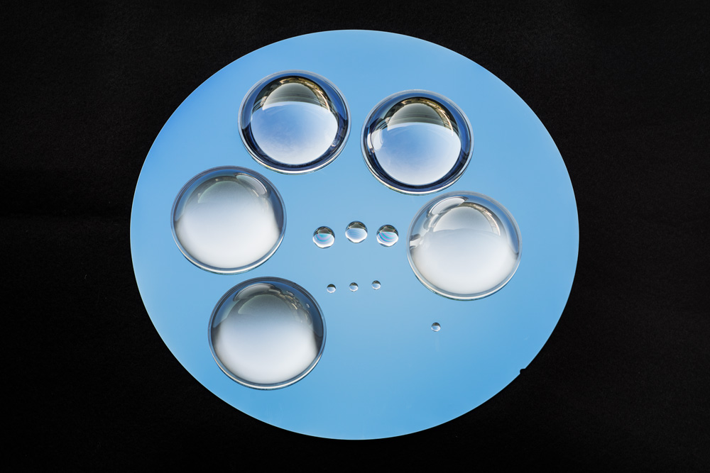
Various optical components functionized by ALD: glass domes with and without antireflection coatings, ball and half-ball lenses with narrow bandpass filter coating.
© Fraunhofer IOF
Fig. 1: Various optical components functionized by ALD: glass domes with and without antireflection coatings, ball and half-ball lenses with narrow bandpass filter coating.
Thickness mapping of a SiO2 ALD thing film with excellent  non-uniformity of ± 0.6 % across a 200 mm diameter area.
© Fraunhofer IOF
Fig. 2: Thickness mapping of a SiO2 ALD thing film with excellent non-uniformity of ± 0.6 % across a 200 mm diameter area.
Al2O3 ALD thin film with tailored mechanical stress by applying bias voltage.
© Fraunhofer IOF
Fig. 3: Al2O3 ALD thin film with tailored mechanical stress by applying bias voltage.


Authors: Kristin Pfeiffer, David Kästner, Vivek Beladiya, Adriana Szeghalmi

3D conformal antireflective coatings by ALD


With ALD (atomic layer deposition) coated lenses.
© Fraunhofer IOF
With ALD coated bald and half-ball lenses.


Antireflective (AR) coatings based on the interference of the reflections at the interface of alternating thin films with low and high refractive indices require precise thickness control. Conventional physical vapor deposition techniques usually produce a non-uniform thickness distribution on strongly curved substrates which severely affects the optical function. We demonstrate the suitability of atomic layer deposition (ALD) to achieve high AR performance even on steeply curved substrates. ALD is based on cyclic self-limiting surface reactions. The thickness of each layer is determined by the number of ALD cycles regardless of the substrate’s shape.

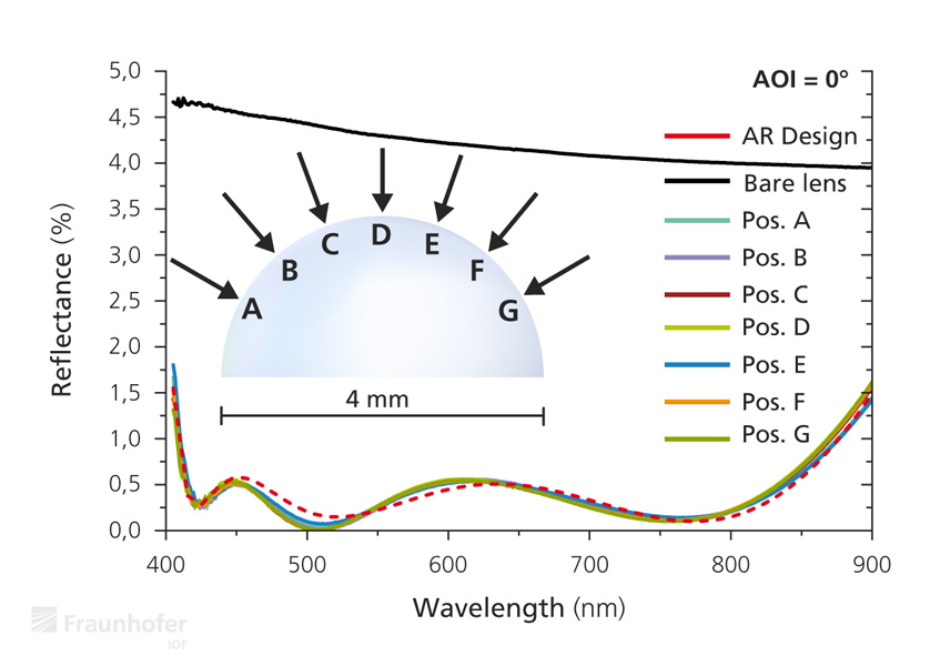
An ALD Al2O3/ TiO2/SiO2-multilayer system has been applied to a fused silica half-ball lens to reduce the reflectance to Rav < 0.3 % in the wavelength range of 390 nm to 750 nm. Excellent agreement of all measured spectra along the lens surface and the design is demonstrated.

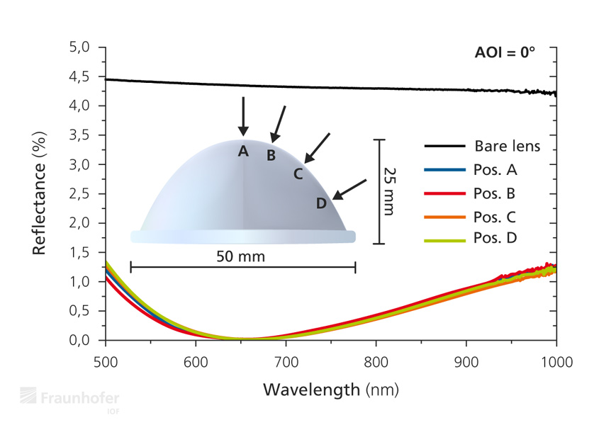
Furthermore, single layer AR coatings consisting of nanoporous SiO2 have been applied. These layers have been realized by the deposition of Al2O3:SiO2 composite materials, where the alumina component was removed by subsequent wet chemical etching. We achieved a conformal AR with Rav < 0.1 % in the wavelength range of 600 nm to 700 nm on an aspheric B270 lens.

Atomic layer deposition is a promising technology for coating thin optical films on complex shaped components, such as convex and concave lenses, cylinders, ball lenses, in tubes or other substrates which are difficult to functionalize precisely with conventional coating technologies.


Highly curved lenses for ALD coating.
© Fraunhofer IOF
Fig. 1: Highly curved lenses for ALD coating.
Chart with the reflectance of an ALD-multilayer AR coated half-ball lens.
© Fraunhofer IOF
Fig. 2: Reflectance of an ALD-multilayer AR coated half-ball lens.
Chart of the reflectance of a nanoporous SiO2 single-layer AR coated aspheric lens.
© Fraunhofer IOF
Fig. 3: Reflectance of a nanoporous SiO2 single-layer AR coated aspheric lens.


Authors: Kristin Pfeiffer, Lilit Ghazaryan, Ulrike Schulz, Adriana Szeghalmi

Conformal nanoporous SiO2 films with tailored refractive index

SEM images of nanoporous SiO2 made by ALD.
© Fraunhofer IOF
Scanning electron microscopy images (top view) of nanoporous SiO2 thin films with approximately 50 % and 70 % porosity, respectively.


Nanoporous SiO2 thin films have attracted intensive research interest for optical applications. Such artificial low refractive index materials are essential for antireflection coatings. In the case of a single layer antireflection coating (SLAR), the refractive index of the coating is equal to the square root of the refractive index of the substrate material. For fused silica and glass substrates, the thin film should have an refractive index in the range of 1.20 to 1.30. Even lower refractive index coatings are required for broadband antireflection coatings. Therefore, various methods have been developed to deposit nanoporous SiO2 thin films such as sol-gel, glancing angle deposition, deposition of mesoporous silica nanoparticles, etc. The precise control of the reflection index and film thickness, and the conformal coating of highly curved 3D shaped substrates such as lenses, cones and cylinders, etc. remains challenging.  In contrast to other coating technologies, atomic layer deposition (ALD) enables conformal coatings with precise composition and thickness control independent of the geometrical shape of the substrate.

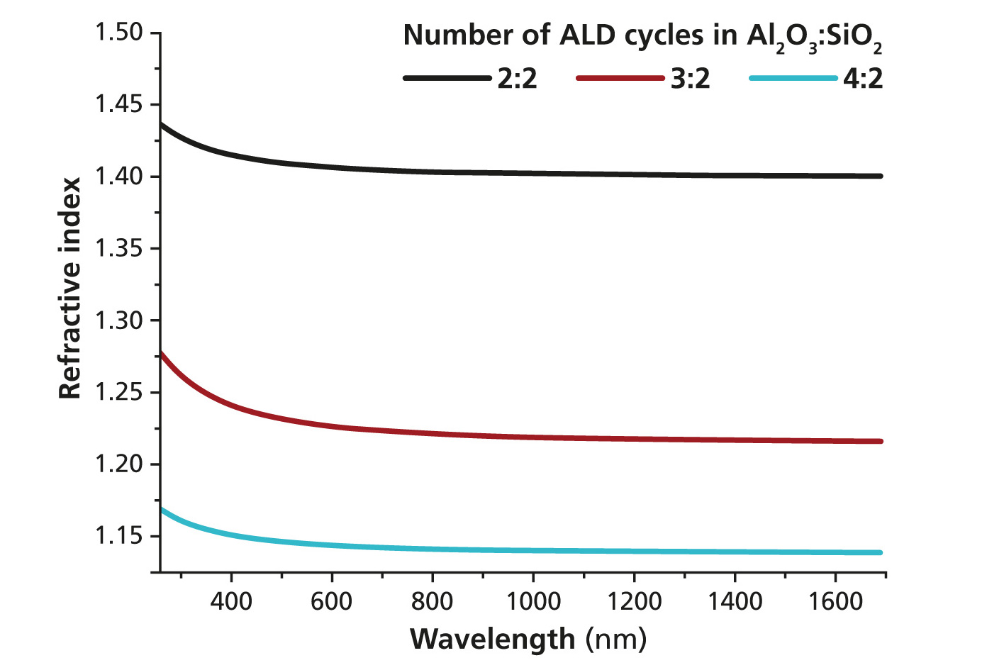
We have developed a new synthetic route for nanoporous SiO2 thin films by atomically mixing SiO2 and Al2O3 followed by selective removal of the alumina constituent. In comparison to other deposition methods, the best results were obtained using ALD which allows precise and reproducible control of the Al2O3:SiO2 ratio in the composites. In general, two ALD-cycles of SiO2 corresponding to approximately 2 Å and two to four ALD-cycles of Al2O3 corresponding to 2 to 4 Å build the basic sequence of the composite materials. The final thickness is achieved by repeating the Al2O3:SiO2 sequence until the desired thickness is reached. By increasing the Al2O3 content, the final SiO2 film porosity has been tailored from 10 % to 69 %, which in turn has resulted in a decrease of the refractive index from 1.40 to 1.15 at 632.8 nm wavelength (Fig. 1).

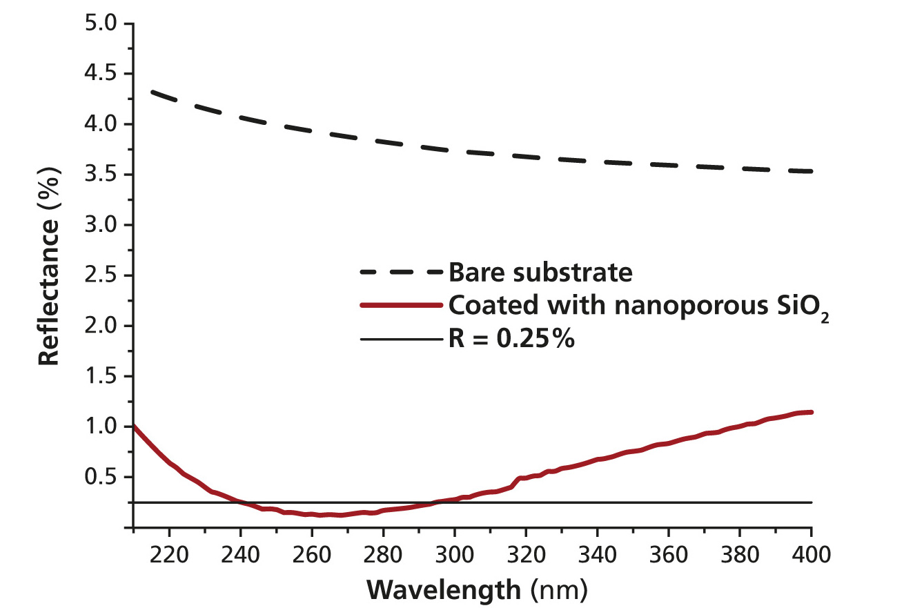
The nanoporous SiO2 films were applied as antireflection coatings on various glass substrates. A single layer antireflection (SLAR) coating for the UV spectral range around 256 nm wavelength was demonstrated using an Al2O3:SiO2 composite with the ALD-cycle ratio 3:2. The control of the film thickness led to the minimum reflectance R at the required wavelength (Fig. 2). Such coatings are designated as top layer for broadband antireflection coatings.


Chart of the dispersion of the nanoporous SiO2 thin films.
© Fraunhofer IOF
Fig. 1: Dispersion of the nanoporous SiO2 thin films.
Chart of SLAR coating.
© Fraunhofer IOF
Fig. 2: SLAR coating on fused silica with Rmin < 0.2 % from 245 nm to 290 nm wavelength.


Authors: Lilit Ghazaryan, Ernst-Bernhard Kley, Adriana Szeghalmi

Atomic layer deposition of antireflection coatings

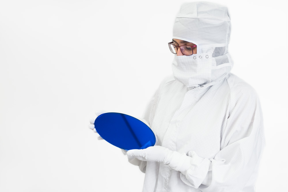
Uniform Al2O3 thin film (ca. 100 nm) on an 6 inch silicon wafer, processed using atomic layer deposition (ALD).
© Fraunhofer IOF
Uniform Al2O3 thin film (ca. 100 nm) on an 6 inch silicon wafer, processed using atomic layer deposition.


The deposition of conformal coatings with a precise thickness is crucial for the production of high quality optical thin film stacks. Conventional techniques such as physical vapor deposition (PVD) are suitable for the deposition of thin films on plane surfaces. However, with PVD a non-uniform thickness is generated on curved surfaces, leading to distortions of the optical function of thin film stacks.

We are establishing atomic layer deposition (ALD) as an alternate method of meeting the high requirements on the thickness uniformity of the single layers and also on highly curved lenses and to control the thickness of optical film stacks without in situ monitoring.

The main advantage of ALD is its capability to deposit conformal coatings on structured surfaces with high aspect ratios. The film thickness is defined exactly by the number of ALD cycles. The deposited layers have a high lateral uniformity and low roughness.

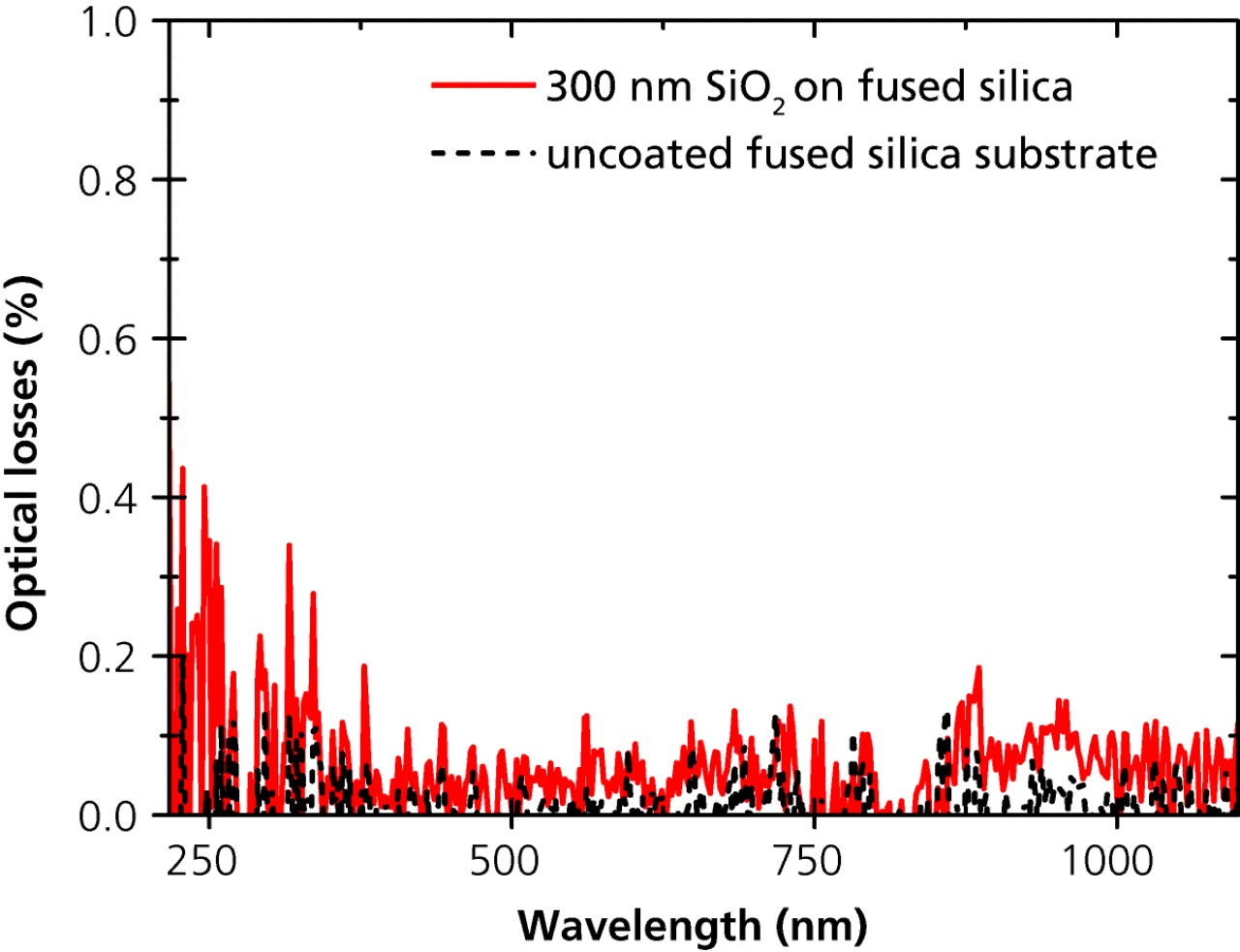
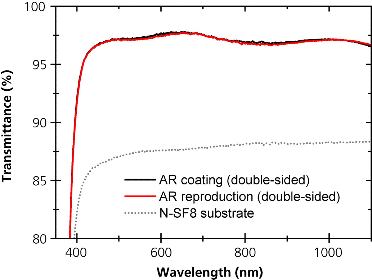
With the developed ALD processes for Al2O3, TiO2, HfO2, and SiO2, we achieve a high reproducibility and a linear growth rate that is necessary for precise thickness control. Our results show that atomic layer deposited films exhibit only little absorption losses down to a spectral range of 200 nm (SiO2, Al2O3), 260 nm (HfO2), and 400 nm (TiO2). Laser calorimetric measurements (λ=1064 nm) of 300 nm films on quartz substrates revealed low absorption values of only 5.4 ppm (TiO2), 3.3 ppm (Al2O3), und 3.9 ppm (SiO2), whereas the substrate itself has losses of about 2.3 ppm. Using the materials SiO2 and HfO2, we demonstrated a broadband antireflection coating for the spectral range of 390 nm to 1100 nm. The thicknesses of the single layers are just controlled by the number of ALD cycles. In further experiments other optical elements such as dichroic mirrors and narrow bandpass filters will be realized.
 

Silicon wafer coated with a homogeneous Al2O3 thin film.
© Fraunhofer IOF
Fig. 1: Silicon wafer coated with a homogeneous Al2O3 thin film.
Chart with low-loss SiO2 coating on fused silica substrate.
© Fraunhofer IOF
Fig. 2: Low-loss SiO2 coating on fused silica substrate.
Chart with measured transmittance of a double-sided broadband antireflection coating on two NSF8 substrates.
© Fraunhofer IOF
Fig. 3: Measured transmittance of a double-sided broadband antireflection coating on two NSF8 substrates.


Authors: Kristin Pfeiffer, Svetlana Shestaeva, Astrid Bingel, Peter Munzert, Adriana Szeghalmi

More scientific publications


In addition, our researchers publish scientific results in scientific journals. A selection list of scientific papers on the subject of atomic layer deposition can be found below:

More information


Further details on atomic layer deposition and our range of services can be found on the following page:


Have we sparked your interest?


Please contact us.

We develop customized solutions for photonic problems from industry and science.

Further information


Possible characterization and material treatments for ALD-coated substrates and components:

  • Spectrophotometry, ellipsometry, XRR, XRD, AFM, SEM, etc.
  • Thermal stability and annealing
  • Chemical stability and wet chemical etching
  • Handling of moisture sensitive substrates under inert atmosphere

More information and services on surface and thin film characterization


Functional surfaces and coatings

Get an overview of all services offered by our scientific department “Functional Surfaces and Coatings” at Fraunhofer IOF.

Overview