CGH Developments

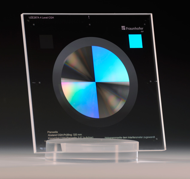
Asphere-Test-CGH based on Effective-Index Structures

Effective-Index of an asphere test-CGH.
© Fraunhofer IOF
Effective-Index of an asphere test-CGH.

Testing of spherical optics is typically performed using interferometric methods. During such a measurement, the surface being tested is illuminated with a spherical wave and deviations of the surface shape from this wave can be characterized by superposition of the reflected light with a reference wave. In recent years, aspherical and freeform optical surfaces have gained increasing importance for the realization of optical systems. For their characterization, the above-mentioned method is no longer suitable as the surface shape inherently deviates from a sphere and no useful information can be extracted from the interfero-metric measurement. In such cases, the use of computer generated holograms (CGH) for adapting the interferometric illumination wave specifically to the optics being tested has been an established method for a long time. Thus, these CGHs represent a ruler for the aspherical surface.The light deflecting structure of CGHs typically consist of a binary grating with locally varying period. Such patterns achieve a diffraction efficiency in the range of 40 %, resulting in an overall light portion of only 16 %, usable for the measurement as the light passes the element twice. The unused light remains in the beam path of the interferometer and can thus interfere with the measurement, or even make it impossible. Higher diffraction efficiencies are achievable e.g. by micro-structures comprising a larger number of height levels (e.g. 4-level elements). Their lithographic realization, however, requires a significantly higher effort and the typical fabrication tolerances are reducing the wave-front accuracy of the CGH.

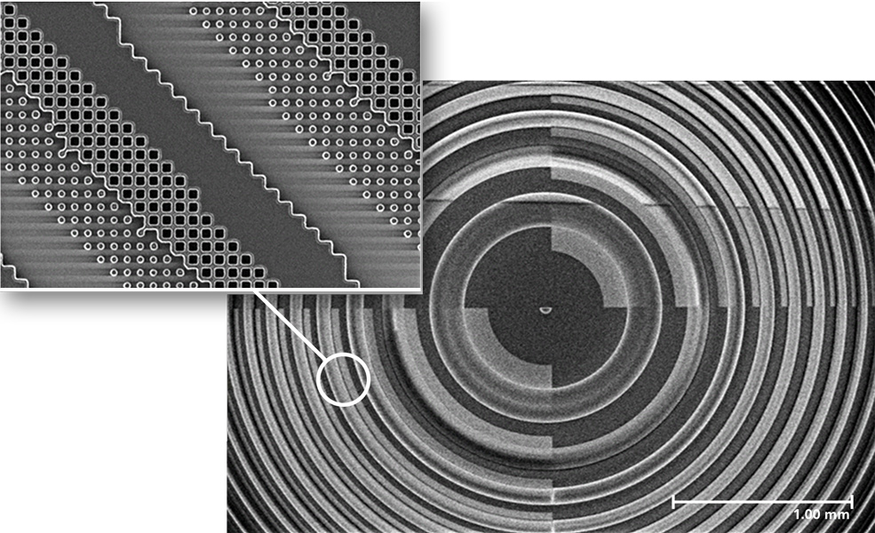
SEM image of the CGH's nano-structure.
© Fraunhofer IOF
SEM image of the CGH's nano-structure.

For the first time, the efficiency improving multi-level function of such an asphere test CGH has been realized by sub-wavelength structures at the Fraunhofer IOF. Because of their small lateral dimensions, the interferometric light does not resolve these structures. Nevertheless, by locally varying the duty-cycle of the structures, a lateral variation of the phase-delay can be implemented. Their optical function is therefore similar to that of a material with locally varying effective refractive index. A great advantage of this realization method for a multi-level structure is the fact that only a binary surface profile is required which is fabricated in a single lithographic patterning step. Consequently, the achievable wave-front accuracy is identical to that of a simple 2-level CGH and the accuracy reduction due to subsequent lithography layers can be completely avoided. The realized test CGH was characterized to show a diffraction efficiency of 76 % in single pass transmission, which corresponds exactly to the theoretically expected value.


Authors: Uwe. D. Zeitner, Frank Burmeister, Thomas Flügel-Paul, Philipp Schleicher, Tino Benkenstein

Design and Manufacturing of Computer-Generated Holograms

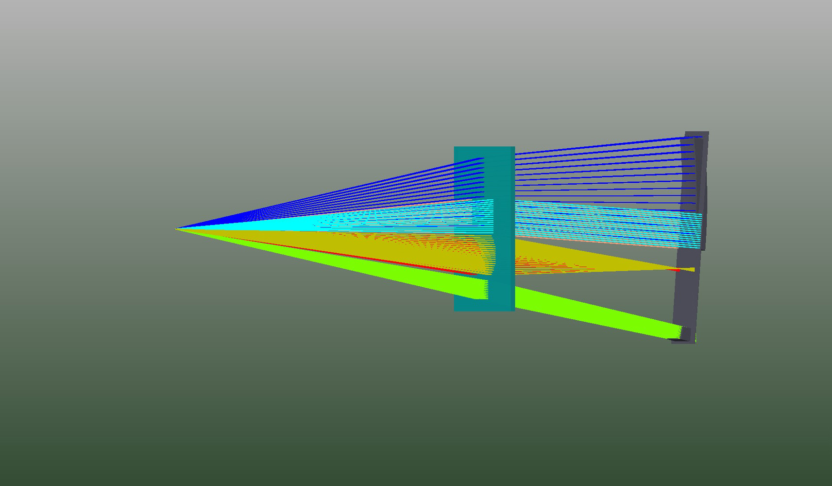
Optical design of a CGH for interferometric testing of a freeform mirror.
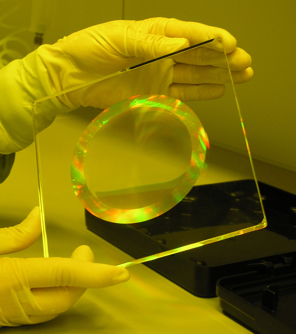
Structured CGH on a 6-inch mask blank (152 mm x 152 mm x 6.35 mm).
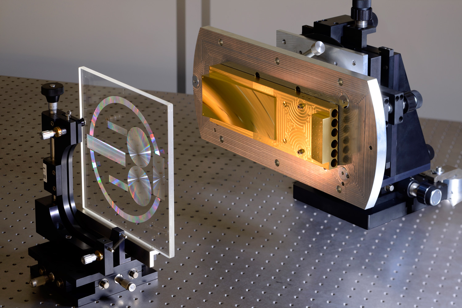
Setup for interferometric testing of a freeform mirror.

Computer-generated holograms (CGHs) allow for contact-free interferometric testing of demanding optical surfaces, for example aspheres or free-forms, with an accuracy < 10 nm RMS. To realize this, a high-precision lithographic fabrication technology and the use of special substrates with sub-100 nm flatness are needed.


Our Offer

  • Optical design of phase functions and layout
  • Provision and correction of substrates (transmitted wavefront error < 10 nm RMS)
  • Lithographic fabrication of CGHs
  • Measurement of placement accuracy
  • Measurement of transmitted wavefront


Lithographic process chain

  • Coating of substrate with chromium and photoresist
  • Exposure by use of electron beam lithography
  • Transfer of structure into chromium mask through reactive ion etching (RIE)
  • Transfer of structure into substrate through RIE
  • Removal of chromium mask (selective removal possible)


Technical Data

  • Available substrate geometries:
  •     6-inch (152 x 152 x 6.35) mm
  •     9-inch (230 x 230 x 9) mm
  •     ET (292 x 150 x 15) mm
  • Placement accuracy < 20 nm (3σ)