 Fraunhofer Institute for Applied Optics and Precision Engineering IOF
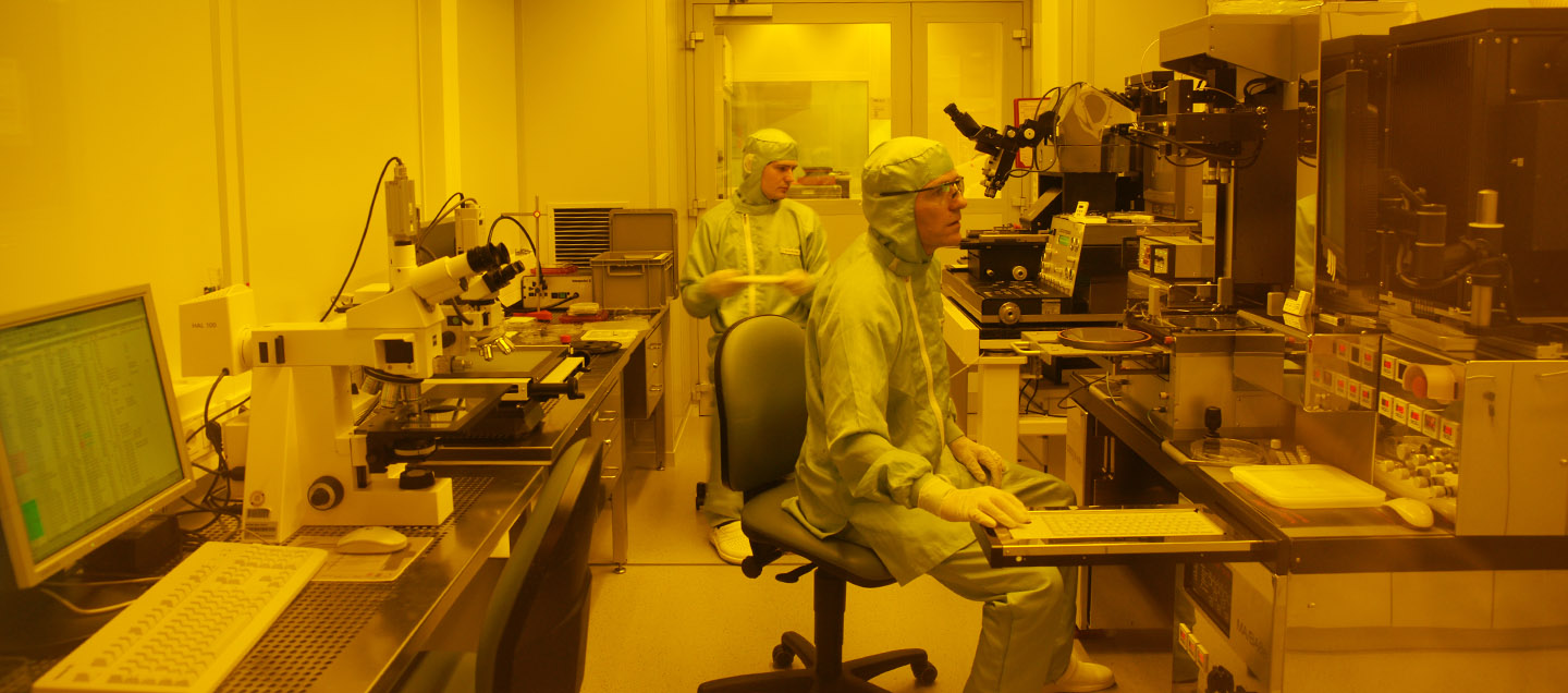
Lithographic processes enable the simultaneous production of a large number of elements with the highest lateral accuracy, a key requirement for micro-optical integrated on wafer scale.
The key technologies are:
- Binary photolithography in contact mask aligners, including use of positive/negative thick resists
- Photoresist reflow; here, binary photoresist structures are formed into precise, lenticular structures, a standard method for generating microlenses
Photolithographically structured polymer or metal layers serve as apertures, reflectors, color filters and as (masters for) binary gratings, diffraction plates, spacers etc.
Reflow structures serves as microlens master structures for diverse molding technologies or are transferred to the underlying glass or silicon substrate through reactive ion milling.
Typical properties/parameters of reflow microlens structures:
- Substrates: 100, 150, 200 mm
- Hardware used: SUSS Microtec MA6, MA8e
- Lateral resolution: ~ 1 µm, lateral adjustment +- 1 µm
- Spherical/toric/cylindrical surfaces
- Accuracy of form achievable at diffraction limit
- Lens arrays with high space factor (> 99 %)
- Lateral dimension: 10 µm...> 1 mm, large structural height possible (> 100 µm)
- Extremely flat contact angle (~ 1°) also achievable
- Conical forms (limited) achievable with special processes
- Any variation of lens parameters (lens profile, size, position, orientation) achievable via the array
- High uniformity across the wafer (+- 1 % fluctuation)
- Production of multifunctional elements by combining lithographic processes