German Future Prizes for Fraunhofer IOF

Disruptive technologies in cooperation with our research institute

Fraunhofer IOF writes success stories


On behalf of industry and research, we not only develop customized solutions, but also realize disruptive technologies that open up access to new market structures for our partners and are decisive for competition.

Discover our innovative capacity by taking a look at the research projects that have been awarded the German Future Prize:

  • 2020 for the development as well as industrial series-production readiness of the EUV technology, which experts consider to be the future standard in industry.
    Read more
  • 2013 for the development of an ultrashort pulse laser (USP laser) for industrial applications – such USP lasers have become an indispensable part of today's series production.
    Read more
  • 2007 for the development of LEDs with particularly high luminance, making them usable as a ubiquitous light source as we know it today.
    Read more


Are you looking for a reliable cooperation partner to support you all the way from the initial idea to its application? Contact us with your request and we will provide you with a solution!
 

Contact us

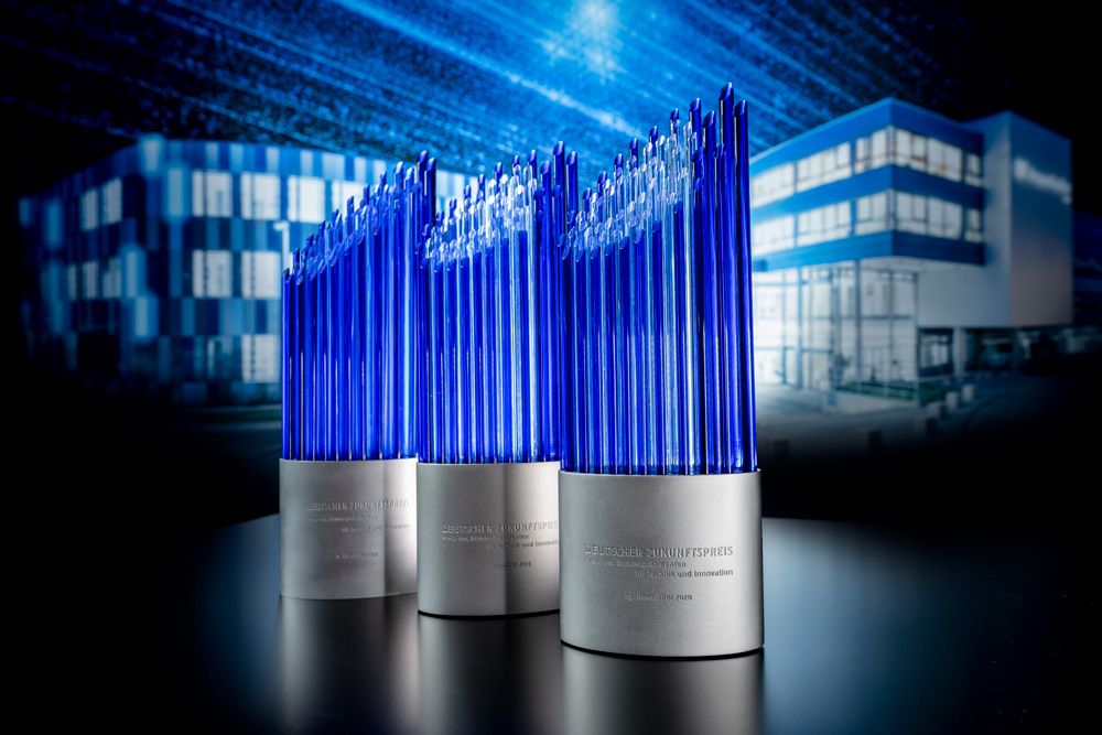
Three trophies of the German Future Prize.
© Fraunhofer IOF
Three trophies - after 2007 and 2013, Fraunhofer IOF 2020 receives Germany's most important research award for the third time.

2020

EUV lithography opens the way to smaller and more powerful microchips


Microchips are the foundation of our digital world. EUV lithography enables the production of even smaller and more powerful chips – for automated driving or state-of-the-art smartphones, for example. Dr. Peter Kürz from ZEISS, Dr. Michael Kösters from TRUMPF and Dr. Sergiy Yulin from the Fraunhofer Institute for Applied Optics and Precision Engineering IOF were awarded the German Future Prize in 2020 for their project "EUV lithography – new light for the digital age".


EUV lithography enables great leaps for digitization


The winning team has made a significant contribution to the development and industrial production readiness of EUV technology. The result is an emerging technology backed by more than 2,000 patents that forms the basis for the digitization of our everyday lives. It enables applications such as autonomous driving, 5G, artificial intelligence, and other future innovations.

The Dutch company ASML is the world's only manufacturer of EUV lithography machines. As an integrator, the company designed the architecture of the overall system and in particular the EUV source. Key components of these machines are the high-power laser from TRUMPF for the EUV light source and the optical system from ZEISS.

EUV stands for "extreme ultraviolet", i.e., light with an extremely short wavelength. This key technology will facilitate the production of far more powerful, energy-efficient, and cost-effective microchips in the coming decades than ever before.

After all, successful digitization cannot be achieved without a further sharp increase in computing power. Today, a smartphone already has millions of times the computing power of the devices that accompanied the first moon landing in 1969. This is made possible by a microchip barely the size of a fingertip, which contains more than ten billion transistors.

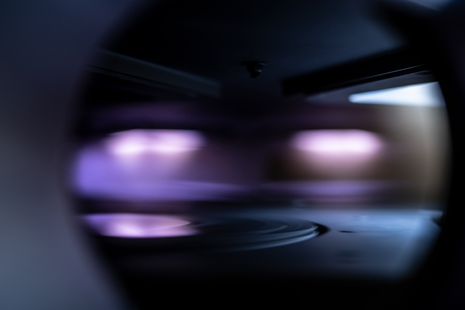
Rotating movements coat the optical components.
© Fraunhofer IOF
View inside the Nessy coating facility at Fraunhofer IOF, where EUV coatings are produced by magnetron sputtering.

EUV light overcomes previous limits of what is technically possible  

The production process for the latest chip generations is based on the use of EUV light, which overcomes previous limits of what is technically possible. Nearly the entire exposure technology had to be developed from scratch, starting with the light source, then the optical system in a vacuum, and finally the surface coating of the mirrors. Fraunhofer IOF was as a key research partner in the sophisticated coating technology for the mirrors.

Together with his research team at Fraunhofer IOF, Sergiy Yulin developed basic principles for the coating design of the collector mirror used in EUV lithography. Yulin and his closest colleagues Torsten Feigl and Norbert Kaiser have succeeded in developing highly reflective precision mirrors with unique optical properties. Their results have laid the foundation for the success of EUV lithography. Their revolutionary layer system was the first to effectively reflect up to 70% of EUV light at temperatures of up to 600 degrees.

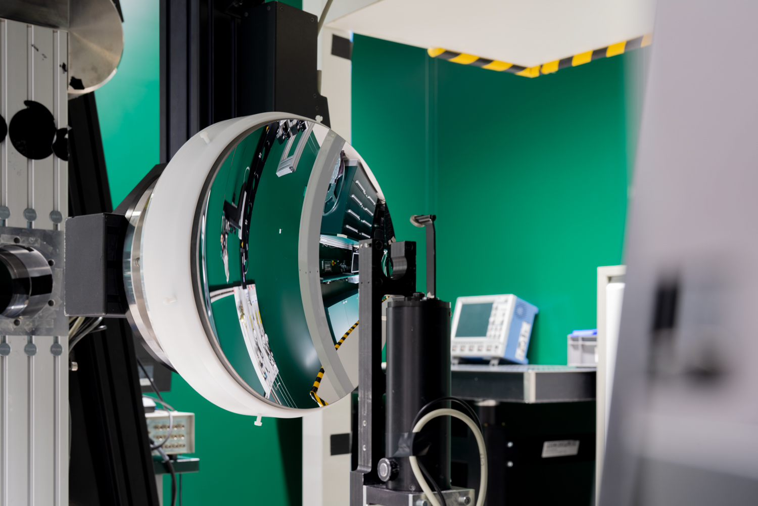
Collector mirrors for extreme ultraviolet lithography.
© Fraunhofer IOF
Collector mirrors for extreme ultraviolet lithography during the characterization process.

The knowledge gained by Sergiy Yulin from the development of highly specific mirror layer systems for EUV lithography can also be used for exciting applications in life and materials sciences. As a result of the EUV lithography project, layer designs and manufacturing processes have been developed that have made the wavelength of 13.5 nm usable for a broad field of research for the first time, for example in biology and medicine. They can also provide fascinating insights into the structural composition of matter and materials in microscopy in the so-called water window, space observation, or spectroscopy in the EUV spectral range.

With the world's strongest pulsed industrial laser, TRUMPF supplies a key component for the exposure of the most modern microchips used in every modern smartphone. There is no economical alternative to this laser for generating the light required for EUV lithography.

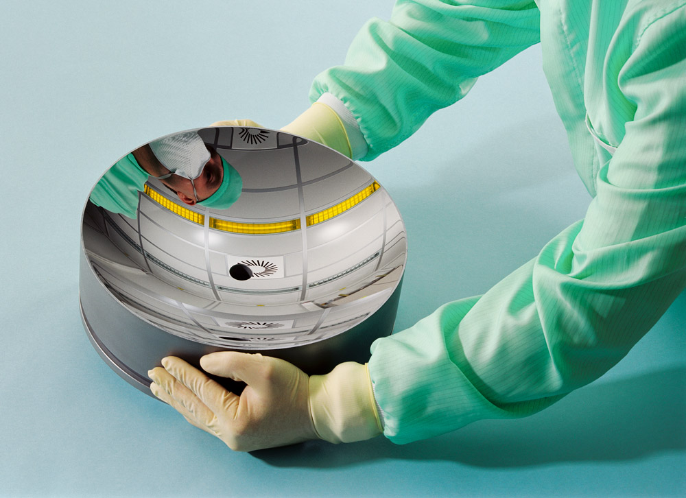
The quality and shape of the illumination system and the resolution of the projection optics from ZEISS determine how small structures on microchips can be. Significant innovations can therefore be found in the mirrors that are inserted into the optics system. Since even the smallest irregularities lead to imaging errors, the world's "most precise" mirror was developed for EUV lithography.

Coated EUV collector mirror from Fraunhofer IOF.
© Fraunhofer IOF
Coated EUV collector mirror from Fraunhofer IOF.

2013

Production with flashes of light: Ultrafast pulse laser for industrial series production


It works precisely, cost-efficiently, and fast - the ultrashort pulse laser. In series production, it is opening new doors with its ability to ensure maximum precision even at maximum productivity. It was developed by employees of the Fraunhofer Institute for Applied Optics and Precision Engineering IOF and the companies BOSCH and TRUMPF. In 2013, Prof. Dr. Stefan Nolte, Dr. Jens König and Dr. Dirk Sutter were awarded the German Future Prize for their world-leading technology.

Areas of application for lasers in industrial production severely limited in the past

Light is used in many ways as a tool in industrial manufacturing processes. In the form of laser beams, it can be used for mechanical work such as cutting, drilling, or welding. For a long time, however, the use of lasers in industrial production was severely limited. The reason: conventional lasers heat up the target material too much - be it metal, ceramics, or plastic. This results in melting the material which then often necessitated costly and time-consuming post-processing.

The ultrashort pulse laser solves the problem of costly post-processing

The light pulses of the ultrashort pulse laser are so short, but so intense, that the materials do not melt, but vaporize. The resulting vapor can then be extracted with pinpoint accuracy. In addition, the pulse duration and energy as well as the focus can be precisely adjusted with the new high-power laser, so that a precise cut through the material is possible. Materials that previously could not be processed with lasers can now also be treated with this method - such as diamonds or sapphires. The laser works completely contactless, so there is hardly any wear. Even with a high number of pieces and the smallest objects of only a few millionths of a millimeter (nanometer), it manages to guarantee a constant and optimal quality. 

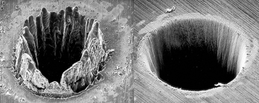
Comparison of two microbore in stainless steel. Left: Pulse duration of 3.3 ns (the edge of the drill hole is frayed and uneven); right: Pulse duration of 200 fs (the edge of the drill hole is smooth and even).
© Fraunhofer IOF
Comparison of two microbore in stainless steel. Left: Pulse duration of 3.3 ns; right: Pulse duration of 200 fs.

The ultrashort pulse laser operates on the basis of a mirror system

This enables computer-assisted laser pulses to be directed to the desired spot. The time required for this process is very short: The laser emits hundreds of thousands of pulses per second. This means that the duration of the pulses is in the picosecond range. That is 10-¹² seconds, or one trillionth of a second. This makes it possible to process the smallest structures - for example, engraving a match head without it catching fire.

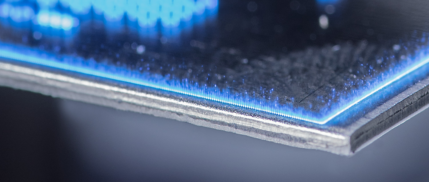
Very small and ultrafast laser pulses are necessary for micromaterial processing. Enhanced phototography to show detailed smallest of laser pulses.
© Fraunhofer IOF
Using very small and ultrafast laser pulses for micromaterial processing

Opening up many new industrial areas of application thanks to basic and applied research

The physical fundamentals of this joint project were researched by Prof. Dr. Stefan Nolte from Fraunhofer IOF and Friedrich Schiller University Jena. This could then be used in an applied manner by colleagues from the companies BOSCH and TRUMPF – Dr. Jens König and Dr. Dirk Sutter. Together, the three thus made the ultrashort pulse laser usable for series production. Previously, these lasers were rarely used outside of research labs. However, there is industrial demand for the technology in the manufacture of screens for smartphones, in applications in ophthalmology, the automotive industry, semiconductor manufacturing, industrial engineering, and the electrical industry, among others.

Ultrashort laser pulses are shown to cut or drill a small surface.
© Fraunhofer IOF
Ultrashort laser pulses enable contactless, high-precision and low-damage processing of almost all materials. With pulse peak power in the gigawatt range, they are ideal for structuring, drilling, cutting, and joining.

2007

From low-light LEDs to high-performance LEDs

LEDs are more durable and energy-efficient than classic light bulbs. However, due to their weak luminosity, they were initially limited in their potential applications. A team of researchers from the Fraunhofer Institute for Applied Optics and Precision Engineering IOF and Osram Opto Semiconductors GmbH finally succeeded in developing high-power LEDs with a particularly high luminance. Dr. Andreas Bräuer, Dr. Klaus Streubel and Dr. Stefan Illek were honored for their work with the German Future Prize in 2007.

Thin-film technology revolutionizes light generation

As a decorative element, for faucets or as background lighting - these used to be the conventional areas of application for light-emitting diodes. The reason: Although the lamps were long-lasting and cost-efficient, their luminance was too weak to be used anywhere that required high-intensity light sources.

It was the development team led by Dr. Andreas Bräuer, head of the former department of Microoptical Systems at Fraunhofer IOF, and Dr. Klaus Streubel and Dr. Stefan Illek from Osram Opto Semiconductors GmbH that unlocked new potential for the application of light diodes. With the help of the so-called "thin-film technology" and special packages and optics, they succeeded in producing LEDs with significantly higher luminance than ever before.

The Fraunhofer IOF team provides the optimal optics

The innovative high-performance LEDs benefit from the close links of solid-state physics and optics. A semiconductor chip is found at the center of a light-emitting diode. When an electrical voltage is applied to this semiconductor, it emits light. The developers optimized the previously low luminance by using thin-film technology: A metal reflector is built into the chip for this purpose, a kind of mirror that leads to higher efficiency.  

Dr. Klaus Streubel and Dr. Stefan Illek from Osram contributed a new chip technology to the development. It allows light to be coupled out in only one direction. Parallelly, a novel package platform for the thin-film LEDs promotes efficient temperature management and the combination of LEDs of different colors. The development of the optimal optics for this system was driven by Dr. Andreas Bräuer and his team at Fraunhofer IOF. They made maximum use of the emitting light with the help of special optics. The researchers designed secondary optics that capture and focus the light emitted by the LED as close to the chip as possible, as well as tertiary optics that homogenize the light beam.

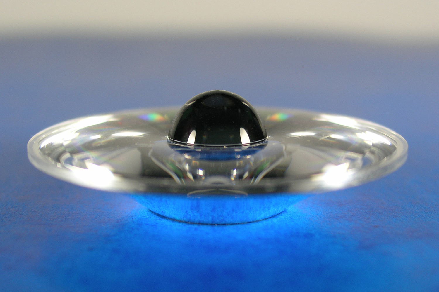
Diamond-turned concentrator reminiscent of the shape of Saturn and its rings.
© Fraunhofer IOF
LED beam shaper: A concentrator manufactured using ultraprecision turning as a secondary optic that concentrates the light emerging from an LED in the desired direction.

More sustainable LEDs find a wide range of applications

Thin-film LEDs are efficient, durable, and robust, converting more electricity into light than any other light source. The now widely banned incandescent bulb managed to convert just 5 percent of the energy that it generated into light. The remaining 95 percent was emitted as heat.

In contrast, the new high-power LEDs enabled efficient light generation, which is now used in car headlights, projectors, and street lighting, among other applications.

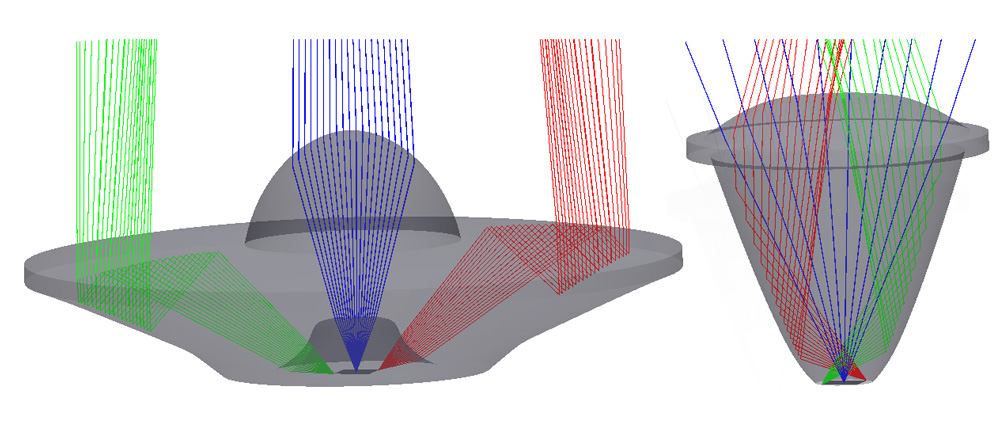
Graphical representation of beam shaping within a concentrator.
Refractive/reflective concentrator: the central light cone of the LED is collected refractively by a lens, while light components with a larger exit angle are guided to the edge of the TIR concentrator and from there are imaged via a ring mirror.
Micro-optical, irregular honeycomb condenserfor segmented and automative LED-high-beams
© Fraunhofer IOF
Segmented automotive LED high beam realized as a micro-optical irregular honeycomb condenser.
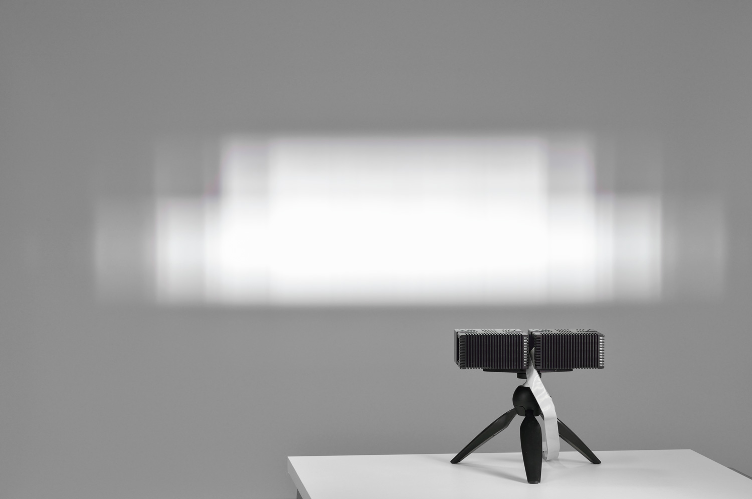
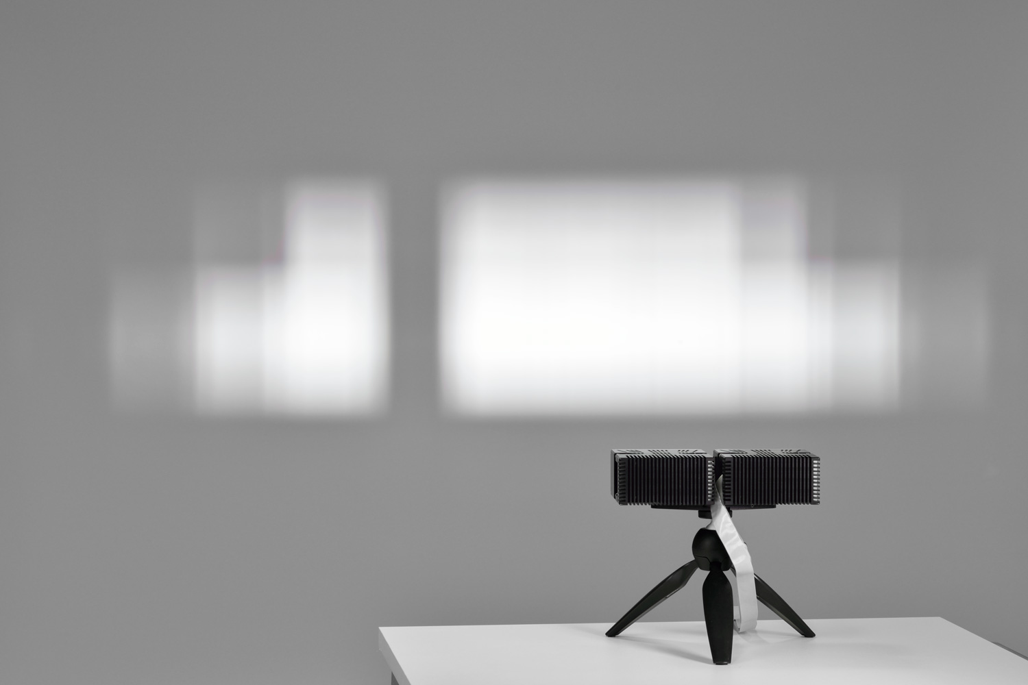
LED projector projects light onto a wall with segments on the left side turned off to avoid blinding oncoming road users.
© Fraunhofer IOF
Individual LED segments can be turned off to avoid glare from oncoming traffic.
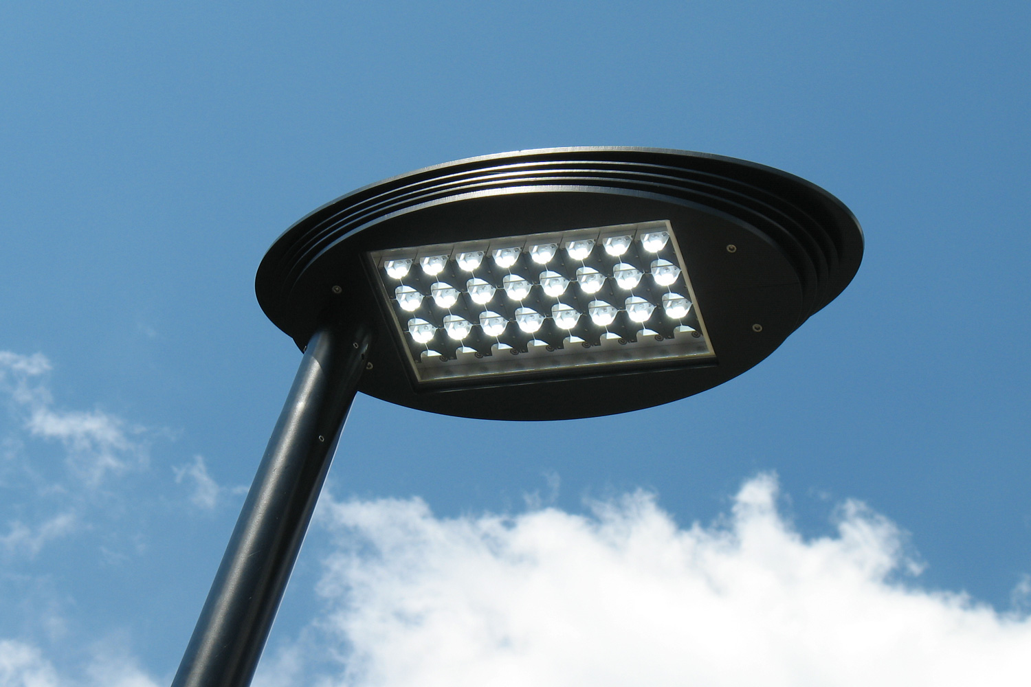
Head of a street light occupied by individual LED reflectors.
© Fraunhofer IOF
Prototype LED street light with free-form reflectors, providing efficient energy utilization.