The implementation of imaging grating elements in low-aberrant spectrometers enables compact, high-resolving optical analytical tools. In particular, all-reflective set-ups according to the Offner concept allow the exploitation of a wide spectral region and are preferentially used in aerospace industry.
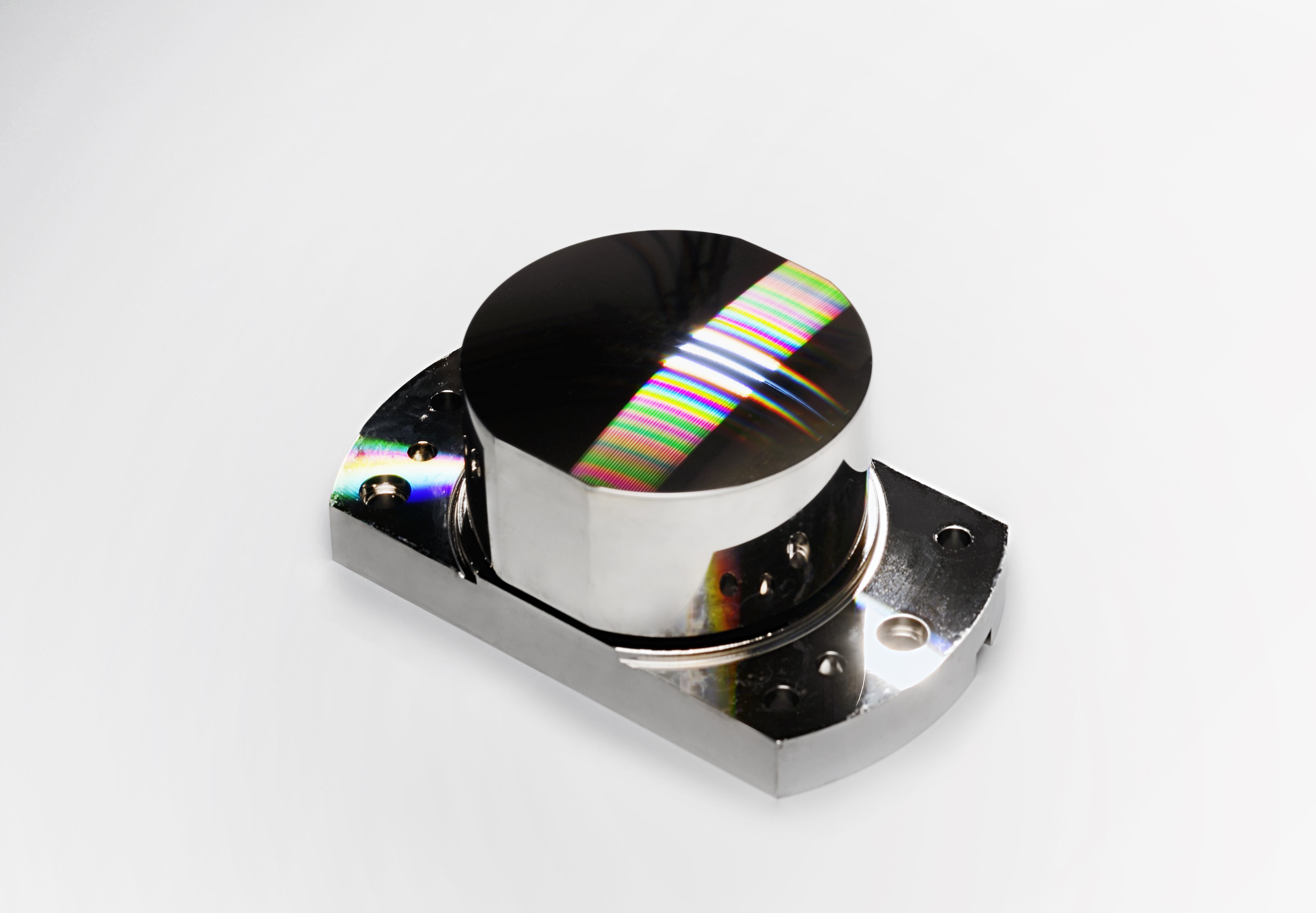
At Fraunhofer IOF, the two structuring technologies single point diamond turning (SPDT) and direct-writing photolithography have been qualified to generate highly-efficient gratings for the visual and near-infrared spectral bands on convex shaped substrates. Within the scope of the development of a spectral resolving satellite remote sensing system (DESIS - DLR Earth Sensing Imaging Spectrometer), binary gratings featuring 13.35 micron period and 137 nm groove depth have been generated onto the convex shaped surface of an aluminum/NiP-substrate. Their radius of curvature was 121.8 mm.
The linear grating is machined using a monocrystalline diamond tool, which cuts directly into the metal surface during an off-axis turning process. As a result of the ultraprecision machining method, a subsequent polishing is not required. The x-ray amorphous structure of the NiP layer allows the formation of sharp-edged grating structures and consequently results in high-contrast diffraction orders.
As alternative technology, the surface has been polished and coated with a photoresist prior to the patterning by direct-writing lithography. The grayscale lithography tool "High Five" is able to dissect the data of the grating pattern of the curved surface into terraces according to the depth of focus of the applied projection optics, and tracks the focus during the resist exposure with respect to the mathematical description of the underlying surface. The grating profile is formed by development and subsequently transferred by reactive ion etching into the substrate.
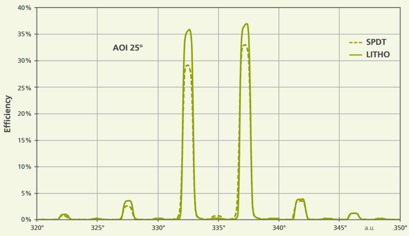
In both cases, a qualified protected silver coating, which has been deposited onto the patterned substrates by magnetron sputtering, acts as a reflector. The first order diffraction efficiency at 25° angle of incidence is 36.5 % and the TE:TM ratio is 1:1 for a wavelength λ = 532 nm.
The activities in this field are continued within the government-funded (federal state of Thuringia) research group "ADONiS" in order to develop novel diffractive optical elements on non-planar substrate surfaces and open them for new areas of application.
Authors: Ralf Steinkopf, Robert Jende, Robert Leitel, Philipp Schleicher, Mark Schürmann
